By using FPGA we can develop reconfigurable wireless sensor network node for transmitting real time data like (temperature, pressure, oxygen level etc.) with low power consumption and high Execution speed, basically wireless sensor node have three different work there are sensing, computing and communicating by using verilog HDL programming language we can program a entire wireless sensor node Architecture, after successfully complete simulation and synthesis or verification we can bout that program into the FPGA board and by using pipelining and parallel processing we can improve the speed of the computing, especially by using hardware acceleration method we can design our WSN different independent block like “sensing block with independent memory - so we can control speed of sensing ability” “computation block with independent memory example - ALU block, Error check block, FIFO registers by using independent block we can improve the flow of execution with high speed and low power ” and “communication block with FIFO independent memory - so we can control the speed of transmitting and receiving with help of PLL” by using this method we can make our wireless sensor node work different mode or different algorithm like “Sleep mode - in this state “sensing block” and “computation block” will stop temporary but still communication block will work because some we need to transmit other node data to another node inside the node there is internal timer will run and it will wake up our node” and “Idle mode - in this state all three block are stop and the internal timer will run and it will wake up our node ”by using these mode we can able to increase the life time of network so it will reduce the Maintenance cost and with help of interfacing LORA wireless communication protocol with FPGA we can do long distance transmit and receive data with low power and it's come under communication block
Project Proposal
1. High-level project introduction and performance expectation
Agriculture is the backbone of India and nearly 70% of people in our country depend on agriculture. The yield of agriculture should be increased rapidly to fulfill the food requirements of the population throughout the world. According to our observation many people are agreed “agriculture is most important thing” and they are willing to do forming by using many different kind of technology like WSN, IOT, AI, ML..etc but the main problem is most of middle class family don’t have money to do this agriculture, because in this agriculture domain IF LAND SIZE IS INCREASED THEN AUTOMATICALLY MAINTENANCE COST AS WELL AS MANAGEMENT ALSO INCREASED
Nowadays Wireless Sensor Network (WSN) is used for solving many real time problems. WSN plays a vital role in many fields like transport, medical, military, mobile phones, home appliances and so on. Agriculture is one of the important sources for all living things. But nowadays agriculture crops are affected due to many environmental changes. To overcome this WSN takes an important role in the field of agriculture. In agriculture WSN is used for monitoring, measuring temperature, irrigation system, measuring water supply and so on. WSN helps the farmer to produce the crop with high quantity and reduce the cost of yield. Agriculture gets affected by climatic change, environmental change, and natural disaster. Using WSN the soil and water management can be done. Here wireless sensors are used so the cost of implementation is very low.
wireless sensor nodes are used to monitor the crops. The temperature, humidity and some other theft detection can be made using sensors. This helps to increase the productivity of agriculture. The human effort is reduced by automatic process and it encourage the farmer to develop the farm land.
FPGA is the one of the flexible technology in digital era because we can develop a WSN by using microcontroller or microprocessor but if we develop our WSN by using microcontroller we can control the functionality of network we can’t alter the architecture of microcontroller but in FPGA - its reconfigurable based on SRAM / BRAM technology so we can develop a entire digital architecture inside the FPGA
According to my knowledge intel is the best offer FPGA for SRAM embedded, high speed transmission logic, best routing, low powered FPGA, i am new to this FPGA so i hope i have a good experience with intel FPGA i heard intel FPGA provide good service and it good for beginners so that why i choose intel FPGA
2. Block Diagram
3. Expected sustainability results, projected resource savings
Without simulating the module i can’t exactly predict performance of network but With respect to hardware accelerators with FPGA intel already done some projects like
-
Intel® FPGA PAC N3000 accelerates network traffic for up to 100 Gbps to support low-latency, high-bandwidth 5G applications. It allows you to create custom-tailored solutions for Virtualized Radio Access Network (vRAN) and core network workloads and achieve faster time to market with the support of industry-standard orchestration and open source tools.
-
Intel® FPGA PAC D5005, previously known as Intel® PAC with Intel® Stratix® 10 SX FPGA, offers inline high-speed interfaces up to 100 Gbps. It allows you to deploy solutions for data center workloads, such as streaming analytics, video transcoding, financial, artificial intelligence, and genomics.
-
Ultrasound, X-ray, CT, and PET applications all require intensive back-end compute operations for algorithms such as fast Fourier transform (FFT) using custom pipeline parallelism. Increased algorithm performance is achieved by off loading from the host processor onto an FPGA
Note - this information collected from intel.com.and based on my research
It is difficult to compare CPU performance against FPGAs. CPU benchmarking is usually specified as how long functions take to execute, and how fast they run whereas FPGA performance is based on data throughput. Modern CPUs run in the order of GHz, as an example a modern CPU might have four cores that run at 2.4 GHz each. Comparatively, speed wise an FPGA is very slow running at just 62 MHz. This looks like a startling difference and might make one wonder, how an FPGA can be fast enough to be of any worth. This is where the parallel processing nature of an FPGA comes in.
Rather than being concerned with how fast an FPGA can run, we are interested in the data rate it can handle. If we take a look at the above image as an example flow of data, we can see how speed is only part of the equation. Data comes into the FPGA, it then gets split up to be parallel processed, the data then feeds into different functions (set up using the logic blocks), in the example we have 6 of these functions. The FPGA then outputs the processed data. This all happens in real time (i.e. a predefined amount of time with only a tiny amount of jitter).
Note - this information is collected from stemmer-imaging.com
FPGA-Based Processor Acceleration for Image Processing Applications
Fahad Siddiqui , Sam Amiri , Umar Ibrahim Minhas , Tiantai Deng , Roger Woods , Karen Rafferty and Daniel Crookes
Received: 27 November 2018; Accepted: 7 January 2019; Published: 13 January 2019
A number of parallel dataflow mapping options were explored giving a speed-up of 8 times for the k-means clustering using 16 IPPro cores, and a speed-up of 9.6 times for the morphology filter operation of the traffic sign recognition using 16 IPPro cores compared to their equivalent ARM-based software implementations. We show that for k-means clustering, the 16 IPPro cores implementation is 57, 28 and 1.7 times more power efficient (fps/W) than ARM Cortex-A7 CPU, nVIDIA GeForce GTX980 GPU and ARM Mali-T628 embedded GPU respectively.
conclution
This are some of my litracter survey based on these report i can predict “hardware acceleoartor will increase the speed of flow of execution”
4. Design Introduction
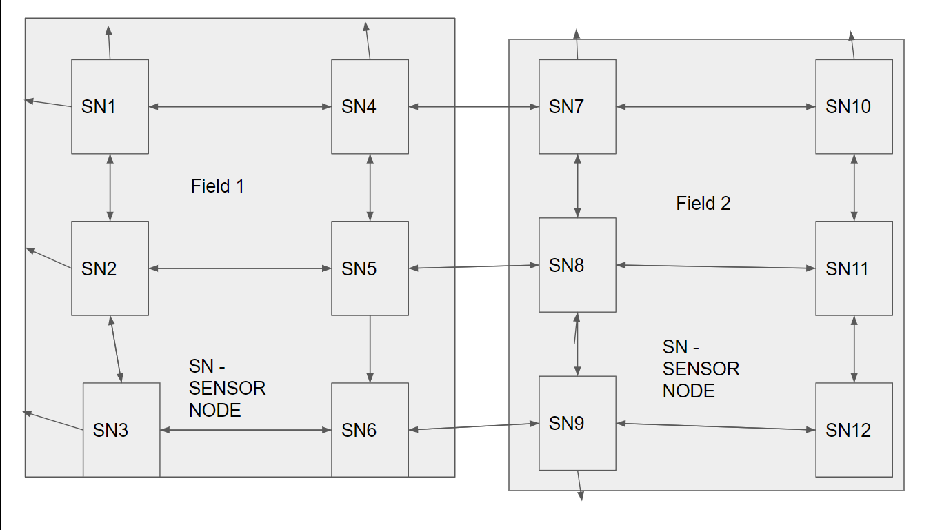
Last 10 years wireless sensor network become booming in all application example military, medical, media, like that scientist and engineers are develop try to different kind of network by using this WSN example standard network, mobile network, etc. and most of the engineers try to implement this WSN in agriculture field
By using WSN in the real field we can monitor our field every second, so that we can collect more data about our field like soil temperature, soil moisture, air temperature and moisture, amount of carbon dioxide in air etc.. based on this data former can understand they field current condition well so they planed they cultivation based on field condition and we can develop and train a Artificial intelligent, machine learning even deep learning also
By using FPGA we can develop reconfigurable wireless sensor network node for transmitting real time data like temperature, pressure, oxygen level etc. with low power consumption and high speed
- basically wireless sensor node have three different work there are sensing, computing and communicating by using verilog HDL programming language we can program a wireless sensor node inside the FPGA board and by using pipelining and parallel processing we can improve the speed of the computing
- expecelly by using hardware acceleration method we can design our WSN different independent block like
- sensing block with independent memory - so we can control speed of sensing ability
- computation block with independent memory example - ALU block, Error check block, FIFO registers by using independent block we can improve the flow of execution with high speed and low power and
- communication block with FIFO independent memory - so we can control the speed of transmitting and receiving operation with help of PLL
- by using this method we can make our wireless sensor node work different mode or different algorithm like
- Sleep mode - in this state sensing block and computation block will stop temporary but still communication block will work because some we need to transmit other node data to another node inside the node there is internal timer will run and it will wake up our node
- Idle mode - in this state all three block are stop and the internal timer will run and it will wake up our node
- with help of these alogorithm we can improve the life time of network and it will decrease the maintance cost
- and interfacing with LORA wireless communication protocol we can do long distance transmit and receive data and it's comes under communication part
5. Functional description and implementation
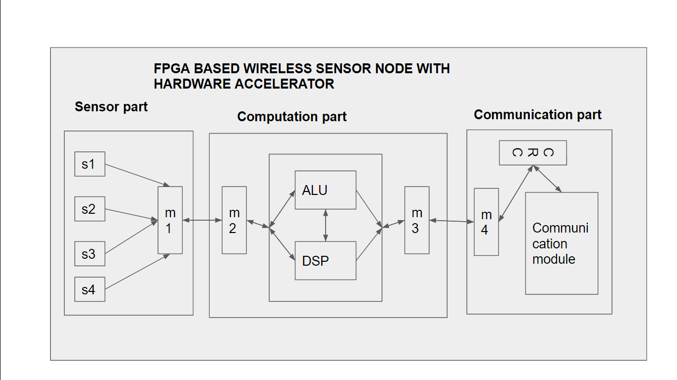
In this wireless sensor node basically divided into three major parts
-
Sensor part
-
computational part
-
Communication part
Sensor part
-
it’s basically collects physical information like temperature, pressure, moisture etc. send that data into specific memory for sensor part
-
That specific memory connected with “slave controller“
-
When sensor data is needed we can collect data from memory with help of slave controller
Computational part
-
It’s fully designed for “computation” purpose like additional, subtraction, multiplication, division etc..this block is know as ALU block and it have DSP block also it will used to signal processing
-
We can fix the threshold value for each sensor computational part will process the sensor value
-
In this computational part there is two master controller
-
One master controller are connect with slave controller which in sensor part when the computational block need’s data it will send request to slave then slave controller from sensor part will transmit that sensor data to computational memory by master controller
-
Another master controller are connect with slave controller which in communication part when computational part need to transmit the sensor data or transmit any signal it will send request to slave controller and send data to communication part memory by using slave controller
-
FIFO memory are used in both side because it will make sure our system work sequential
Communicational part
-
In this communication part is the interface with the wireless communication module (a kind of mixed signal circuit which has a filter, amplifier, antenna etc.”
-
In this part we have slave controller which is connected with computational part
-
After data is processed in computational part then it will transmit that data into this communication part
-
There is separate CRC block or parity block and it will generate error detection or error correction code then our communication part will transmit that whole data through wireless with help of wireless module
-
If any receive from external node then the CRC block will check error detection if the error is occurred then automatically communication part will send ack to that external node
-
In this communication part there is another block “PLL: which is controlled by computational part
-
And in this communication part also we use FIFO memory for synchronous the blocks
6. Performance metrics, performance to expectation
Compared to high-end processors and ASICs the clock speed of FPGAs is low. With this limitation, there is also a loud shout-out for FPGA hardware acceleration from hardware engineers. The configurable features are the most appealing factor of FPGAs, followed by reduced power consumption and performance. Few other notable merits of FPGA hardware acceleration are:
-
Increased parallelism- Multiple tasks from a single application can be run simultaneously. Demanding computational tasks can be solved without consuming much time by incorporating FPGA boards for task migration.
-
Expandable size of data- In FPGAs, the number of bits in the operands in an arithmetic operation can be changed based on requirements. This expansion of the bit size allows any change in the data amidst programming.
-
Suitability for prototyping and validation- The reconfiguration property of FPGAs are well-utilized for prototyping ASICs and SoCs, as they get permanently configured once fabricated. The FPGA prototype is built and validated before starting ASIC fabrication.
The dynamic reconfiguration possibility in FPGA has increased its utilization in electronics, communication, automobile, and aerospace environments. The recent FPGA technology releases incorporate processor cores, artificial intelligence processing units, and Digital Signal Processing ❲DSP❳ chips as a move to transfer a good share of workloads onto FPGA boards. The optimized-FPGAs are becoming more energy-efficient, with increased speed and memory. The influence of customizable computer hardware is growing tremendously, and in-depth knowledge of FPGA boards will help you to design and implement FPGA hardware accelerators.
7. Sustainability results, resource savings achieved
8. Conclusion
0 Comments
Please login to post a comment.