With Moore's Law at its limits, one way of increasing compute capacity is Application Specific Hardware Acceleration; whereby a compute intensive problem is off-loaded to an Application Specific Processor - often called an ASIC - that leverages a specialized data-path to solve the problem much faster than a General Purpose Processor. (Examples are GPUs, Broadband Processors, AI acceleration chips etc.) Problem is, there can only be so many ASICs on a device deployed on edge. Also, ASICs are expensive to produce, and by nature, not reconfigurable.
The Goal of this project is to find a compromise between the expedient, but inflexible ASIC; and the versatile, but slow GPP. The R2A2 will use the Cyclone-V SoC, to realize a general-purpose, single-board, edge-deployable computer, which will run various compute intensive tasks of different resource load requirements. Depending upon the application running at a time, the R2A2 will configure the FPGA component of the Cyclone V SoC to act as an accelerator. This accelerator will be seen by Linux running on the SoC's ARM processor as a separate device, and a corresponding device driver, also loaded on the runtime will interface between the Processor and the FPGA.
By introducing runtime reconfigurable application-specific hardware, the R2A2 will help reduce carbon footprint by reducing global ASIC production requirements: This will eliminate potential e-waste down the years, while still providing high performance per-watt, which is desirable for computing on the edge. Also, high compute power on edge will lift bandwidth strain from the cloud/IoT infrastructure and reduce latency between the systems. Ideally, R2A2 will serve as a prototype for a plethora of Edge/IoT solutions utilizing FPGAs on SoCs for low cost, high flexibility, application specific operations.
Project Proposal
1. High-level project introduction and performance expectation
Motivation
The idea of using specialized computing hardware to solve specific computing problems is by no means a novelty. It traces its history from Intel’s math co-processors, to instruction set extensions like MMX and ARM’s Jezelle, to the now-ubiquitous Graphics Processing Units. More recently, the advances in Machine Learning have introduced AI accelerating hardware in form of ASICs (Application Specific Integrated Circuits), which are fast becoming the norm in mobile platform. These ASICs employ tailor-made data-paths to perform data-manipulation in the optimized matter – just as required by the specific application at hand.
However, the usage of these ASICs (or any application specific computing paradigm) comes at a steep cost. For one, the process of fabrication is long, expensive and needs significant pre-planning. Secondly, due to fast changing application requirements, ASICs aren’t future proof: a truly Application Specific solution may become obsolete as soon as the application changes. Owing to this, the ASICs being fabricated today are never truly Application Specific; instead, they tend to provide a common denominator to many problems in their specific domains.
Of course, there is also the logistical limit of ASICs placed on a single module; one can only have so many packaged ASICs on a circuit board. And even then, a lot of application specific hardware often sits idle for large chunks of time, while the general purpose processor (GPP) wrestles with a novel problem in an un-optimized way.
General Concept
The aim of R2A2 is to mitigate these problems. Utilizing the inherent versatility of an FPGA bearing SoC, the R2A2 will provide a framework for using run-time configurable hardware accelerators for different applications on the go.
The FPGA on SoC will take the form of a pre-synthesized application specific accelerator, based on the application currently being run. The GPP will direct the FPGA based accelerator to perform the resource intensive tasks. Once a new application begins, the FPGA will be reprogrammed, and a new accelerator loaded as per need.
A compact driver being run on embedded Linux will interface with the FPGA-based accelerator, construing it as a regular hardware device, and pass on requisite information and data pointers over the Cyclone-V SoC’s L3 switch.
Application Scope
For the scope of this competition, the project will entail the optimized deployment of at least three resource-intensive compute-on-edge applications with edge-based decentralization and cloud-connectivity as their focus. These applications could be from following domains:
1. Bio-medical Image Processing.
2. Acoustic signal Acquisition and Processing.
3. Edge-Optimized Convolutional Neural Network.
For each of these domains, a tailor-made accelerator will be developed and implemented. It will then be run in conjunction with the GPP, with a hopeful demonstration of clear speed-up over the traditional, GPP based solution.
For every domain-specific accelerator, the following design steps will be followed:
1. Implementation of conventional algorithm to be run on ARM processors.
2. Identification of opportunities for acceleration: Hot-loops of code, common cases, data-manipulation or DSP related compute intensive applications.
3. Design of FPGA based algorithms for previously identified acceleration opportunities.
4. Description of Hardware Blocks in an HDL (Verilog/VHDL/Spinal HDL).
5. Design of HW/SW interface for the accelerator, and its accompanying device driver as a Linux Kernel Module.
6. Integration of the GPP/Accelerator combine and analysis of speed-up.
Relevance on the Edge
This paradigm of compute acceleration essentially attempts to make the common-case fast. With specialized accelerators, we can hope to achieve better Performance/Watt metrics, that is, lower operating power and clock frequencies, as compared to traditional, GPP only edge solutions. Furthermore, high-performance compute capability on the edge will result in high level of decentralization, lower latencies, and lesser burden on cloud-connectivity.
The acceleration architecture, being implemented on FPGA and connected on the cloud, will also allow online performance upgrades and application scope extension capabilities, in form of new or enchanced netlists, downloaded over the internet.
On an environmental level, it will eliminate potential e-waste by replacing obsolescence-prone ASICs with re-programmable application specific hardware, and save planetary resources by obviating excess production of stop-gap ASICs.
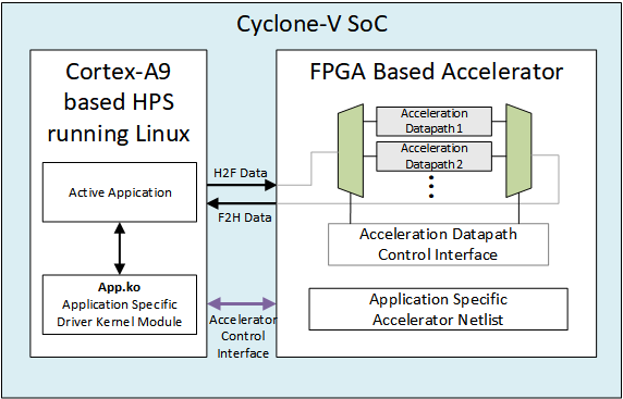
2. Block Diagram
3. Expected sustainability results, projected resource savings
As discussed under the 'Relevance on the Edge' sub-heading, this project has tons of optimization, and resource saving potential. However, solid metrics will only be achieved once a comparison of our design is made with existing solutions. Indeed, a comparison of this sort is one of the objectives of this project.
4. Design Introduction
5. Functional description and implementation
6. Performance metrics, performance to expectation
7. Sustainability results, resource savings achieved
8. Conclusion
0 Comments
Please login to post a comment.