
EM070 » New FPGA family for CNN architectures: High-Speed Soft Neuron Design
Who doesn’t dream of a new FPGA family that can provide embedded hard neurons in its silicon architecture fabric instead of the conventional DSP and multiplier blocks? The optimized hard neuron design will allow all the software and hardware designers to create or test different deep learning network architectures, especially the convolutional neural networks (CNN), more easily and faster in comparing to any previous FPGA family in the market nowadays. The revolutionary idea about this project is to open the gate of creativity for a precise-tailored new generation of FPGA families that can solve the problems of wasting logic resources and/or unneeded buses width as in the conventional DSP blocks nowadays.
The project focusing on the anchor point of the any deep learning architecture, which is to design an optimized high-speed neuron block which should replace the conventional DSP blocks to avoid the drawbacks that designers face while trying to fit the CNN architecture design to it. The design of the proposed neuron also takes the parallelism operation concept as it’s primary keystone, beside the minimization of logic elements usage to construct the proposed neuron cell. The targeted neuron design resource usage is not to exceeds 500 ALM and the expected maximum operating frequency of 834.03 MHz for each neuron.
In this project, ultra-fast, adaptive, and parallel modules are designed as soft blocks using VHDL code such as parallel Multipliers-Accumulators (MACs), RELU activation function that will contribute to open a new horizon for all the FPGA designers to build their own Convolutional Neural Networks (CNN). We couldn’t stop imagining INTEL ALTERA to lead the market by converting the proposed designed CNN block and to be a part of their new FPGA architecture fabrics in a separated new Logic Family so soon.
The users of such proposed CNN blocks will be amazed from the high-speed operation per seconds that it can provide to them while they are trying to design their own CNN architectures. For instance, and according to the first coding trial, the initial speed of just one MAC unit can reach 3.5 Giga Operations per Second (GOPS) and has the ability to multiply up to 4 different inputs beside a common weight value, which will lead to a revolution in the FPGA capabilities for adopting the era of deep learning algorithms especially if we take in our consideration that also the blocks can work in parallel mode which can lead to increasing the data throughput of the proposed project to about 16 Tera Operations per Second (TOPS).
Finally, we believe that this proposed CNN block for FPGA is just the first step that will leave no areas for competitions with the conventional CPUs and GPUs due to the massive speed that it can provide and its flexible scalability that it can be achieved from the parallelism concept of operation of such FPGA-based CNN blocks.
Many AI designers and developers wish one day to build or test their own convolutional neural network architectures in addition to other AI blocks and systems on a hardware platform like FPGA due to its impressive high-speed and parallel computation capabilities but what about creating a new family of FPGA just for this purpose? I mean a new family of FPGA that has the maximum silicon fabric architecture optimization to perform the Artificial Intelligence operations exceptionally regards to the ultra-high computational speed that it can provide in comparing with other hardware platforms like CPU, GPU and even the conventional types of FPGA chips in the market today while providing a huge amount of flexibility in comparing to the ASIC solutions that were provided by Google and intel and other companies.
This project is the start trigger to reflect the dreams into reality by introducing a new concept in FPGA architecture silicon fabric. The future of this project aims to replace the conventional DSP blocks by Neuron blocks in a new type of FPGA families, I call it “HORUS FPGA family”, but the recent goal is just to prove the concept by designing and implementing a proposed single neuron using an authentic and genuine closed source VHDL-based architecture and no third-party IP used at all.
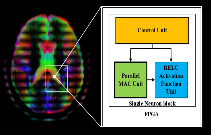
Fig. 1 The figure reflects the main idea behind the this project
During the first testing stage of the proposed simplified neuron unit, the computational speed performance reached up almost 5 Giga Operation per second (5 GOPS) for each single neuron when it was tested on Stratix V 5SGXEABN3F45I3YY FPGA chip and it will be left for the reader the computational speed that this proposed project can achieve by adding thousands of parallel neurons and what will be the performance of this new generation of HORUS FPGA family in the CNN data processing if it adopted by Intel Altera. SO far, the modified MAC unit (or the MPA unit) is designed and tested, and it achieved a maximum operating frequency up to 834.03 MHz in Arria 10, and about 454.13 MHz for Cyclone IV E. I reached a design of the MPA unit that could perform up to 123 simultaneous operation per clock cycle, but in this project, I presented the simplified MPA unit that can perform up to 5 operations per clock. Again, I will let the door open to the reviewer to imagine to how much we could boost the overall system performance if all the DSP bocks in the new FPGA family generation replaced with this neuron blocks. It will be so excited to many users in many different fields to use this new FPGA architecture that will start a new era of creativity in the field of artificial intelligence in general and CNN in specific.
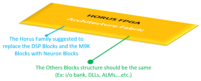
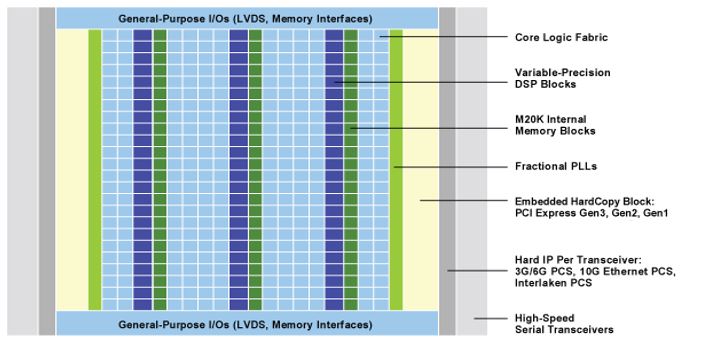
Fig. 2 Block diagram of Altera's Stratix V FPGA
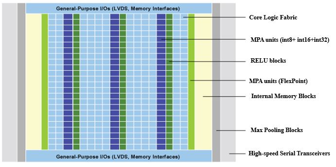
Fig. 3 Block diagram of The proposed FPGA Silicon Architecture
In order to finalize this project, some software tools and hardware kits have been used as the following:
Software Tools:
(Used for the VHDL coding description of the project)
(used in the verification stages: functional simulation of the design)
(used for the project synthesis and also for timing analysis and power analysis)
Hardware kits:
(the FPGA in which the code has been implemented on it)
(used as the interface module between a PC and the FPGA board)
The proposed project block diagram will be consisting of two main sub-blocks, as in the figure below. The first sub-block, is the neuron block, which includes the proposed novel high-speed parallel Multiply Parallel Addition (MPA) [ which is the replacement of the conventional Multiply-Accumulate unit (MAC)], RELU activation function, and a control unit using Finite State Machine (FSM) that control the flow in the neuron unit and the ability to interface it with the HSSC unit. The second sub-block, is the High-Speed Serial Communicator (HSSC) block which is a serial interface block that gives the testability of the proposed neuron using a GUI interface software.
System block diagram:
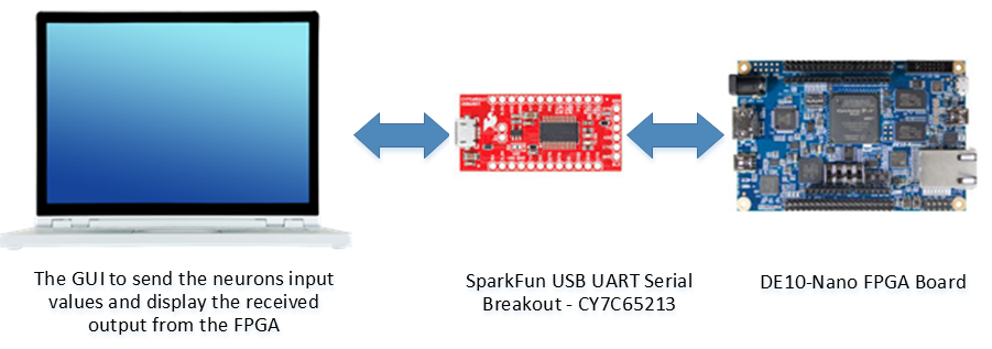
Fig. 4 The generic system diagram of the proposed system
Project block diagram:
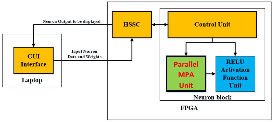
Fig. 5 The detailed system diagram of the proposed system
The custom neuron architecture in this project gives us the power to create many featured upon the requirements, which in deed helped to boost the overall system performance. The first achievement so far is that each single neuron can operate with a speed up to 5 Giga Operation per second (5 GOPS) using Arria 10, which gives us the vision of what will be the overall performance when combining hundreds or thousands of neurons to operate together, shortly, the speed of computation can reach up to tens of beta Operation per Seconds (TOPS), which one of the reasons to select FPGA as the optimum hardware-platform for such project oriented purposes in comparing with CPUs or GPUs hardware-platforms solutions nowadays. Also, this project can work as the accelerator unit in cooperate with the conventional CPUs and GPUs as well.
By using VHDL coding and by building all the design elements from scratch gives seamless features’ control capabilities when the proposed neuron where designed, one of these features is the ability of the periodic repetitive operation every clock cycle due to the tailored finite state machine controller in this system so, every clock cycle, the neuron unit could process the data input values in addition to their corresponding filter weight coefficients and fire the output.
Also, as it well known that each CNN architecture, such as LeNet, AlexNet, GoogleNet, ResNet has a different number of input dendrites which triggered an essential request to take in the consideration that the proposed design should adopt to this scalability issue, which is already have been solved by 2 methods; the first one is by adjusting the FSM unit to allow more MPA units to be combined; or by redesign a larger MPA units as it has been demonstrated in the future work section and proved in the first 3 published scientific papers in the References section, and again both the solution presents a novel way to overcome the related issues.
For system testability feature, the HSSC unit was designed from scratch using VHDL codes to receive the input data and their corresponding weights coefficients from a computer software and forward the computed neuron output to the computer software to display it. The designed HSSC is full custom peripheral interface that using UART protocol and it can achieve 2.5 Mbps data transfer rate. As a conclusion, the whole codes required to build such system is totally genuine and no third-party IPs used. Also, the HSSC can be expanded to be an array of HSSC to achieve more transfer data rates inside the proposed AI framework (this is future feature to be added).
Despite the fact of the outstanding performance of using the deep learning networks in a wide range of academic and industrial applications related to computer vision to natural language processing, the reduction of the processing time of the tremendous number of computational elements required in such networks still one of the hot research areas nowadays. Many research contributions had been done so far to accomplish the optimum utilization performance without causing any observable degradation in the overall efficiency, especially for the Convolution Neural Network architectures such as LeNet, AlexNet, GoogleNet, ResNet.
The most influential factor that directly affects the overall performance of the deep learning networks is the massive number of two vectors dot product units needed to be executed in each layer of these networks. Several researches proved that optimizations can be reached through the dependence of high speed hardware accelerator platforms such as Field Programmable Gate Array (FPGA) and Application Specific Integrated Circuits (ASIC), regarding to their capabilities to provide adaptable and parallel processing architectures in comparing to other hardware platforms such as Center Processing Units (CPU) and Graphic Processing Units (GPU). Also, other research contributions demonstrated that replacing the floating-point based architectures for designing the deep learning networks, with an 8-bits fixed-point architecture can attain almost the same computational performance.
The two vectors dot product is achieved in digital design using the multiply–accumulate operation (MAC) unit, which computes the product of two operands and adds/subtracts that product to the accumulated result stored in the accumulator. The impact of designing an optimized MAC unit is directly enhance significantly the overall speed performance and the data throughput of the deep neural network architectures. Many FPGA vendors such Intel Altera, equipped their FPGA Integrated circuits (IC) with dedicated generic architecture features, such as the variable-precision Digital Signal Processing (DSP) blocks and the embedded memory blocks to boost the speed performance of implementing the MAC operations needed in a wide variety of digital application processing units such as High-Precision Fast Fourier Transforms (FFTs) units, and High- Precision Finite Impulse Response (FIR) filters. On the other hand, Xilinx proposed their UltraScale Architecture DSP48E2 primitive DSP Slice, which provide a high speed overall performance to fit many DSP applications units as fixed and floating point Fast Fourier Transform (FFT) functions, Systolic and MultiRate FIR filters. To enhance the Xilinx DSP48E2 DSP utilization resources, it has been suggested to add Lookup table (LUT) units to maximize the operation density for the 8-bit operands, which considered a remarkable solution toward increasing the overall computation performance for the Xilinx FPGAs only.
Tailoring properly the generic DSP blocks to fit the deep learning networks architecture aimed to be designed, is considers as one of the main issues of the previously suggested solutions, which leads to either wasting the chip resources or increasing the confusion due to the massive amount of unnecessary details in each DSP block, especially when designing complex neural networks. Also, the dissimilarity of the DSP block between FPGA vendors, make the flat switching from one vendor to another, or from FPGA to ASIC design a harsh situation. In this project, a proposed full custom parallel MAC unit has been designed using VHDL to overcome these issues by using LUT-based architecture, in which there is no dependence on neither the DSP features nor the embedded memory blocks provided on the FPGA architecture fabric.
In fact, this project is depending in a new idea which is not only to replace the conventional MAC units in the FPGA silicon fabric, but also to add the RELU activation function at the end of the proposed MAC unit to form a complete neuron unit. Also, the proposed neuron unit increases the number of operations per clock cycle for the same required task and attaining almost a computational performance capability that achieved 3.13 Giga Operation per Second (GOPS) for each individual neuron unit and this value can be increased if we targeted a high-density FPGA family. It is really interesting to see this project, which is still under its first steps to be an end product especially if we replaced the 8-bits signed number format with the state of the art number format, Flexpoint, from Intel into such project.
5.1. Proposed System Description
The convolutional layer is considered as the most demanding layer comparing to the other layers in any convolutional neural network architectures for its massive computational processing requirements due to the enormous number of multiplier and addition blocks needed to achieve the dot product functionality. Conventionally, the dot product functionality in the convolutional layer was attained using sequential MAC unit design such used in CPU or GPU hardware-based systems or by non-optimized parallel MAC unit in FPGA hardware-based systems due to the dependency of the hard DSP units in its silicon fabric.
In general, the FPGA hardware-based systems are the optimum solutions from the computational speed point of view due to the design architecture flexibility and the parallelism capability offered by such platforms. The proposed parallel MAC unit is designed to boost the computational processing speed performance of the convolutional neural network by depending on a parallel and full-custom MAC unit to perform the two vectors dot product required in the CNN architectures, based on VHDL language, while keeping the independent to the FPGA silicon fabric as one of its main goals to overcome the issue raises when transferring the design from FPGA family to another due to the parameter variations of the generic DSP block in each FPGA family.
The dot product of two vectors can be simply represented as the summation of the element-wise multiplication of these two vectors. So, if the first vector is x= [x0, x1, x2, ……., xn-1], and the second vector is y= [y0, y1, y2, ……., yn-1], and both the two vectors have the same vector length n, hence, as in (1), the result of the dot product operation on these two vectors can be given as:
x . y = xT y (1)
The dot product is considered as the dominant operation in designing a deep neural network. To speed up the convolutional layer computational time using FPGA, a summation of multi-parallel dot product operation between a group of the input feature map element values and the filter weight coefficients is taken place to produce the proposed parallel MAC unit. In this project, a full custom MAC unit with 4 input feature map elements, has been designed and combined with the RELU activation function to produce a complete neuron unit. The proposed MAC design has mainly 3 stages, as shown in the Figure below. In the first stage, four 8-bits elements from the input feature map are extracted and to be multiplied with the corresponding four different 9-bits weight coefficients, extracted from the weight bank, concurrently. The four results from the multiplier units from the first stage will be then added simultaneously. Finally, the result from the addition stage is being accumulated. The output of the proposed MAC unit operation can be described mathematically as indicated in (2), where x is indicating the feature map element values, and y indicating the filter (weights) coefficient values.
Fig. 6 The Proposed 8-bits fixed-point MAC unit
Fig. 7 The Proposed neuron unit ( MAC unit + RELU activation function)
5.2. Proposed Design Verification
For more verifications of the proposed system, a functional simulation has been made using ModelSim SE/PE 5.5e tool. The simulation shows the values of the 4-inputs data (named from r0_0 to r0_3), the 4-inputs filter coefficients (named from w0 to w3), the 4 outputs of the parallel multiplication units (named from x0 to x3), and the final output of the RELU unit (named relu_out). Two identical figures have been included below to make it easy for the readers to understand the results of the simulation (one of them shows the values in Binary, and the other one is shows the values in Decimal or Unsigned).
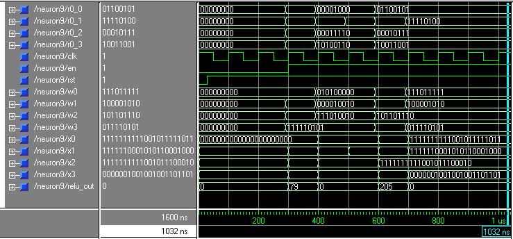
Fig. 8 This Figure describe the Binary values of the proposed neuron results for different scenarios
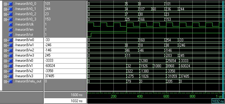
Fig. 9 This Figure describe the Decimal values of the proposed neuron results for different scenarios
Each (They are identical as it has been mentioned before) figure covers all the expected scenarios of the proposed neuron output and in order to make the results readable for the reader, the figure that shows the results in decimal has been reedited and divided into six regions as shown below. The regions are divided as the following:
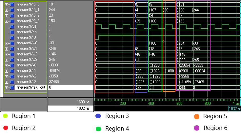
Fig. 10 This Figure describe more illustrative detailed explanation of the proposed neuron results for different scenarios
The proposed neuron unit has been synthetized using Intel Quartus Prime and has been also analyzed for better realization of the three main aspects for a digital design which are the logic utilization, timing performance, and the power consumption. The logic utilization flow summary of the proposed neuron unit, as indicated in the Figure below, showing that proposed neuron unit is occupying about 0.868 % of the total ALMs available on the Cyclone V 5CSEBA6U23I7DK FPGA chip which reflects the ability of the proposed designs to expand the proposed architectures hierarchy for adopting additional multiply-parallel addition units for improving the parallel computation performance efficacy of the systems. Also, the logic utilization flow summary of the proposed design proved that the design architecture is not depends on either the embedded DSP blocks nor the embedded memory bits available in the FPGA silicon architecture, to avoid the dramatic issues and the degradation of the system performance that follows transferring the design among FPGAs with different families, or from different vendors.
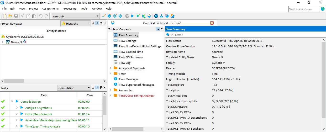
Fig. 11 The Proposed 8-Bits Fixed-Point Neuron Unit Flow Samurry Report
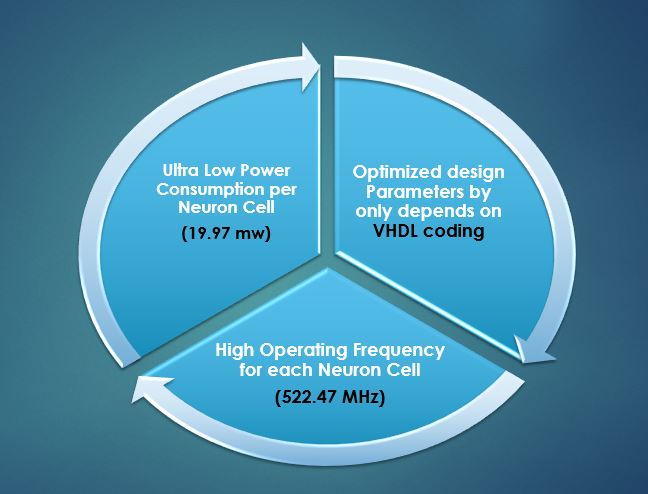
The power analysis as shown in the power analysis figure below, using Power Analyzer tool showed that the core dynamic thermal power dissipation of the proposed neuron unit is only about 19.97 mW and for sure this value will be proportional to the number of the multiplier units in the first layer of the design architecture.
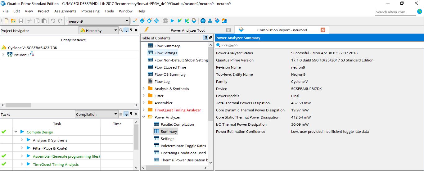
Fig. 12 Power Analyzer Report Of The 8-Bits Fixed-POINT Neuron Unit Using QUARTUS II PowerPlay
For the Timing analysis of the proposed neuron unit, the TimeQuest timing analyzer tool provided by the Quartus Prime 17.1 tool has been used to get the expected timing features of the design and also to check whether the neuron unit will pass the timing requirements of it will fails. The results from the timing analysis showed that the proposed neuron unit has been passed all the timing restrictions successfully and can reach a maximum operating frequency of 522.47 MHz and with a positive slack value in the critical path in the design for both the setup time and hold time as shown in the below figures.
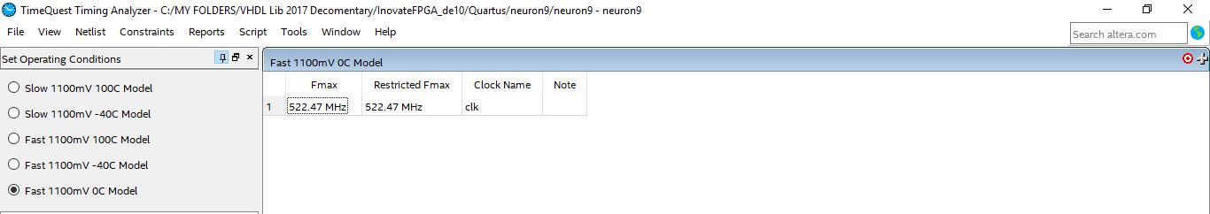
Fig. 13 Maximum freq. result from the time analyzer report of the 8-Bits Fixed-Point Neuron unit Using QUARTUS Prime TimeQuest
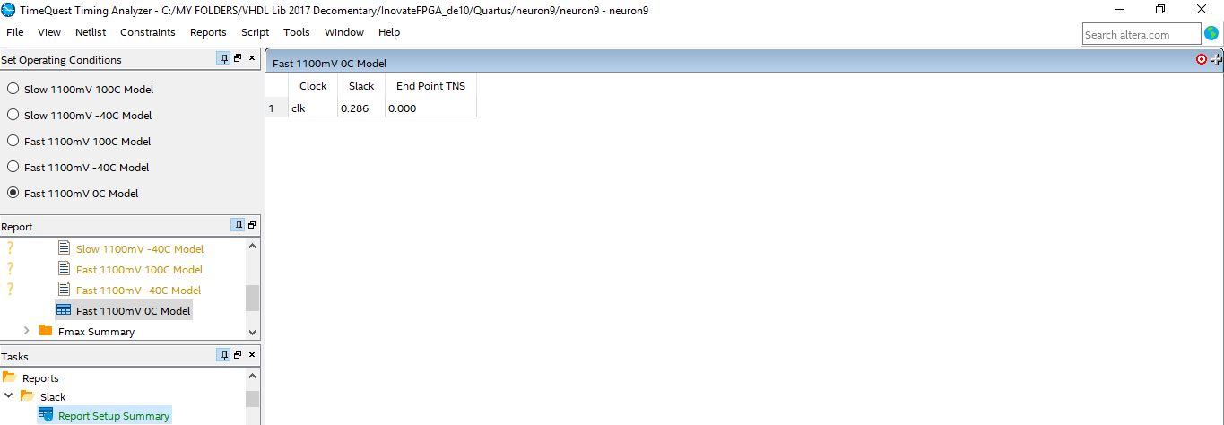
Fig. 14 Setup time result from the time analyzer report of the 8-Bits Fixed-Point Neuron unit Using QUARTUS Prime TimeQuest
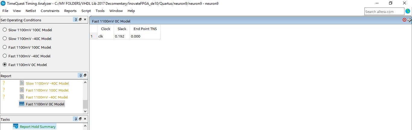
Fig. 15 Hold time result from the time analyzer report of the 8-Bits Fixed-Point Neuron unit Using QUARTUS Prime TimeQuest
As a conclusion of the giving results we can achieve a highest computational performance of 3.13 GOPS using pipelining despite it was expected to achieve 5 GOPS due to the FPGA family used in this project is not designed for high computational performance systems such as Aria 10 or Stratix V, but still the result gives a promising computational speed performance value on low-cost FPGA with a low power consumption as well in which it can be considered as a positive point that the proposed design can be able to work in the applications that required low-power processing end-units such as in IoT and WSN applications.
In the below table we will find a comparision of the proposed neuron unit using different catergories of FPGA familes with the targeted Cyclone V family for giving a wide scope of understanding the computational performance of the proposed system in different FPGA hardware environments.
Table I Computational performance comparison of the proposed system in different FPGA hardware environments
|
|
INTEL ALTERA FPGA Families |
|||
|
Cyclone IV E |
Arria 10 |
Stratix V |
Cyclone V |
|
|
Device |
EP4CE115F29C7 |
10AX115R4F40E3SG |
5SGXEABN3F45I3YY |
5CSEBA6U23I7DK |
|
Total logic elements |
1076 / 114,480 LE ( < 1 % ) |
370 / 427,200 ALM ( < 1 % ) |
356 / 359,200 ALM ( < 1 % ) |
364 / 41,910 ALM ( < 1 % ) |
|
Total memory bits |
0 / 3,981,312 (0 %) |
0 / 55,562,240 (0 %) |
0 / 54,067,200 (0 %) |
0 / 5,662,720 (0 %) |
|
Embedded multiplier 9-bit elements or DSP blocks |
0 / 532 (0 %) |
0 / 1,518 (0 %) |
0 / 352 (0 %) |
0 / 112 (0 %) |
|
Maximum frequency |
454.13 MHz |
834.03 MHz |
815.00 MHz |
522.47 MHz |
|
Setup time Slack |
0.198 ns |
0.051 ns |
0.023 ns |
0.266 ns |
|
Hold time slack |
0.188 ns |
0.065 ns |
0.184 ns |
0.192 ns |
|
Core Dynamic Thermal Power Dissipation |
65.71 mW |
61.62 mW |
55.13 mW |
19.97 mW |
1) System design flow:
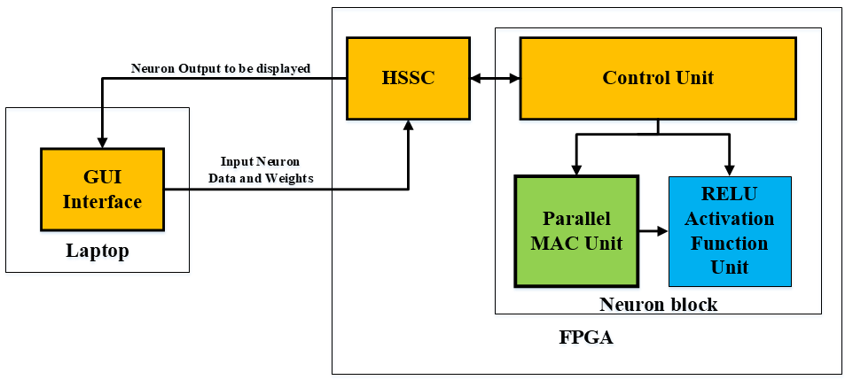
Fig. 16 system design flow which has been illustrated in Fig. 5 above
2) Hardware design block diagram:
Fig. 17 Neuron unit hardware block diagram ( MACunit + RELU unit unit)
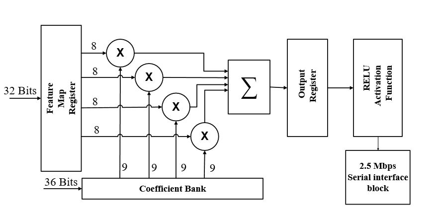
Fig. 18 Final hardware block diagram ( neuron unit + 2.5 Mbps serial interface unit)
3) software flow
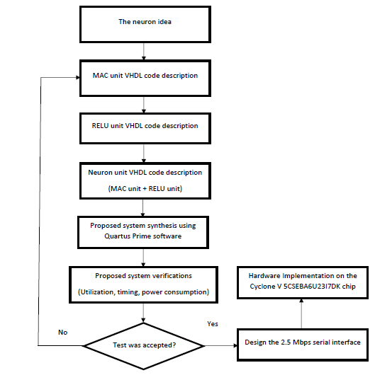
Fig. 19 software flow chart
4) Practical Image from the Hardware Demonstration Video
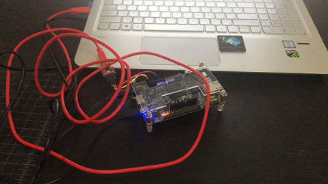
Fig. 20 Practical Image from the Hardware Demonstration Video
8. Future Work
As I mentioned in my recent 4 scientific papers (see the reference section for more details) this year, especially the 3rd paper, that creating a new FPGA chips and their corresponding FPGA Families that have a tailored silicon structures that can give them the adaptability to enhance the new era of accelerating Artificial Intelligence algorithms and especially the Convolutional Neural Network (CNN)- based systems is a mandatory situation that need to be taken urgently in the consideration.
The idea and its implementation in this project can just be considered as only the core of an ambitious and complex set of innovative ideas that will be revealed by the soon future toward achieving a recognized footprint in the AI acceleration systems based on FPGA and ASIC due to the magnificent high-speed capabilities that they can be provide in comparing to the other hardware platforms as CPU or the GPGPU.
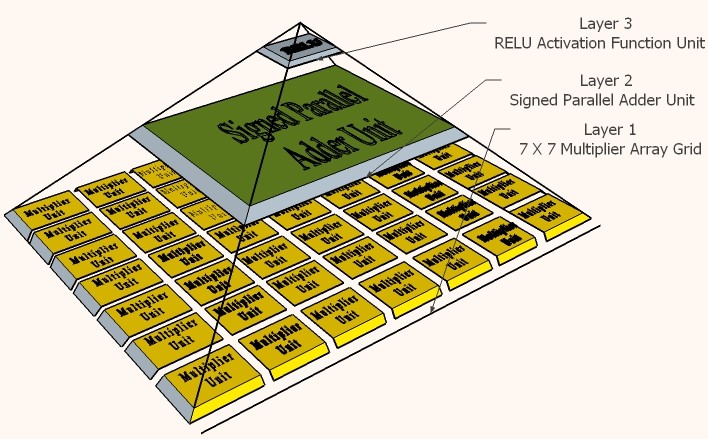
One of the future work that this project can be upgraded with is the proposed pyramidal neuron architectures presented in the 3rd paper in the reference section, that can be used to accelerate the different deep neural network algorithms. The main concept that the proposed three pyramidal neuron architectures relied on for accelerating the computational speed is the parallelism capability provided by using the Field Programmable Gate Array (FPGA) as the targeted hardware platform. Each of the three-pyramidal neuron architecture has different spatial dimensions that depend on the common weight filter sizes in the Convolution Layer of the convolutional neural networks, which are 3X3, 5X5, 7X7. The proposed pyramidal neuron architectures are designed based on an 8-bits fixed point numerical format using VHDL language and are consist of three hierarchical layers. The computational throughputs of the proposed pyramidal neuron units can achieve up to 19.98 Giga Operation per Second (GOPS) in the 7X7 pyramidal neuron architecture using the high-density Stratix V FPGAs. The main reason of the high speed computational performance of the proposed systems is directly related to the replacement of the conventional Multiply Accumulate (MAC) unit, by the proposed Multiply Array Grid (MAG) units and the Multiply Parallel Addition (MPA) units.
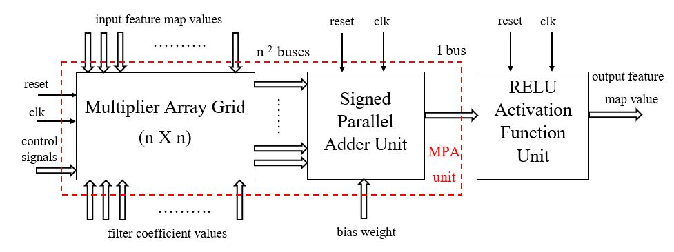
Fig. 21 Generic pyramidal neuron architecture block diagram
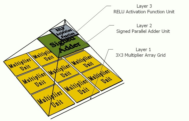
Fig. 22 Graphical hierarchy representation of the proposed pyramidal neuron architecture using the 3x3 multiplier array grid unit
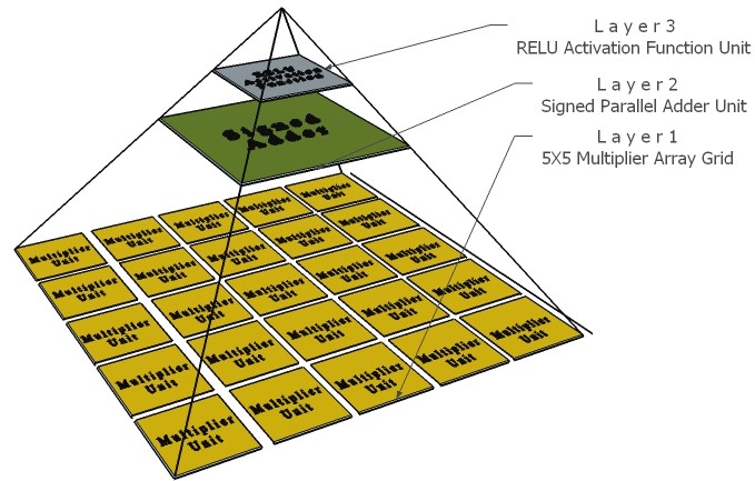
Fig. 23 Graphical hierarchy representation of the proposed pyramidal neuron architecture using the 5x5 multiplier array grid unit
The effect of logic utilization, power consumption, and timing for the 3x3, 5x5, and 7x7 MAGs were deeply covered in last 2 papers (Ref. 2 and Ref. 3) and the next two Paragraphs explain how the size of the 3x3, 5x5, and 7x7 MAGs relate to the bit depth coefficients and input feature map values, which we will find out that both of them are fixed and independant in all of them.
The proposed three pyramidal neuron units have been synthetized using Intel Quartus Prime, and the targeted FPGA chip was Stratix V 5SGXEABN3F45I3YY. The logic utilization flow summary of the three pyramidal neuron units’ comparison, as in Table II, showed that they are sharing some common parameters such as; the activation function type, which is the rectified linear unit; the number of soft addition unit, which is equal to one; also proved that the three architectures don’t rely on either the embedded multiplier 9-bit elements, DSP blocks, or the embedded memory bits available in the FPGA silicon architecture, to avoid the dramatic issues and the degradation of the system performance that follows transferring the design among FPGAs with different families, or from different vendors.
Also, the proposed three pyramidal neuron units proved a reasonable matter, in which the number of logic resources increases as the soft multipliers in the Multiplier Array Grid (MAG) increases, since the amount of logic utilization for the first design consumed is 729 ALM divided into 1455 Combinational ALUTs and 326 for the dedicated logic registers. For the second neuron design, the amount of logic utilization consumed is 2237 ALM divided into 4444 Combinational ALUTs and 972 for the dedicated logic registers, while the third neuron design unit consumption of logic utilization is 4199 ALM divided into 8387 Combinational ALUTs and 1811 for the dedicated logic registers. Also, the results from the flow summary report showed the high efficiency system logic occupation achieved for the three neuron architectures, since the first neuron architecture occupy only 0.203% from the overall logic elements allocated in the Stratix V 5SGXEABN3F45I3YY FPGA silicon fabric; while the second neuron architecture occupy only 0.623% from the overall logic elements; and the third neuron architecture occupy only 1.17% from the overall logic elements, which reflects the ability of the proposed designs to expand the proposed architectures hierarchy for adopting additional multiply-parallel addition units for improving the parallel computation performance efficacy of the systems.
TABLE II. FLOW SUMMARY REPORT COMPARISSION BETWEEN THE THREE PYRAMIDAL NEURONS PROPOSED DESIGNS USING QUARTUS II SOFTWARE
|
|
1st Neuron Design |
2nd Neuron Design |
3rd Neuron Design |
|
Filter Size |
3X3 |
5X5 |
7X7 |
|
Activation Function used |
RELU |
RELU |
RELU |
|
No. of Soft Multipliers |
9 |
25 |
49 |
|
No. of Soft Addition unit |
1 |
1 |
1 |
|
INTEL ALTERA Family |
Stratix V |
||
|
Device |
5SGXEABN3F45I3YY |
||
|
Logic Utilization (in ALMs) |
729 / 359,200 |
2,237 / 359,200 |
4,199 / 359,200 |
|
System Logic Occupation |
0.203% |
0.623% |
1.17% |
|
Combinational ALUTs |
1455 |
4444 |
8387 |
|
Dedicated Logic Registers |
326 |
972 |
1811 |
|
Total Memory Bits |
0 / 54,067,200 |
0 / 54,067,200 |
0 / 54,067,200 |
|
Embedded Multiplier 9its Elements or DSP Blocks |
0 / 352 |
0 / 352 |
0 / 352 |
The second critical aspect that needed to be analyze is the timing performance, which influenced by maximum cycle time that the system can reach without surpass the limitation of the hardware platform. The time analysis for the proposed neuron architectures was accomplished using the TimeQuest Timing Analyzer tool provided by Intel Quartus Prime software under the following environment assumptions; the input netlist assumed to be post-fit; the delay model is fast-corner; the operation condition was selected to be Min_fast_900mv_0C. As indicated in Table II, the first neuron with the 3X3 multiplier array grid achieved a maximum operating frequency of 474.38 MHz, and the maximum operating frequency for the second neuron with the 5X5 multiplier array grid obtained 526.32MHz, while the maximum operating frequency for the third neuron with the 7X7 multiplier array grid obtained 391.70 MHz.
It was predicted that the first neuron design will obtain the greater operating frequency above which the second and the third neuron can achieve due to the less number of the multipliers it has in the multiply array grid (MAG) layer, but the results showed that it achieved a maximum operating frequency lower than the value achieved by the second neuron design which has 5X5 multipliers in its multiply array grid (MAG) layer. Also, as an explanation of the reason behind the low obtained maximum frequency that has been achieved by the third neuron design, in comparing with the other two neuron designs, is due to the larger number of multipliers it has in the multiply-array grid (MAG) layer, which causes a more efforts in routing the network to connect of the sub-blocks it has, especially the clock network.
Table III Time Analyzer Report Comparision Between The Three Pyramidal Neurons Proposed Designs using Quartus ii TimeQuest
|
|
1st Neuron Design |
2nd Neuron Design |
3rd Neuron Design |
|
Filter Size |
3X3 |
5X5 |
7X7 |
|
INTEL ALTERA Family |
Stratix V |
||
|
Device |
5SGXEABN3F45I3YY |
||
|
Latch Clock Name |
Clk |
Clk |
Clk |
|
Maximum Frequancy |
474.38 MHz |
526.32 MHz |
391.70 MHz |
|
SDF clock constrains |
clock period = 2.2 ns Freq = 454.54 MHz Duty Cycle = 50% |
||
|
Setup Time Slack |
0.092 ns |
0.300 ns |
-0.353 ns |
|
Hold Time Slack |
0.200 ns |
0.177 ns |
0.201 ns |
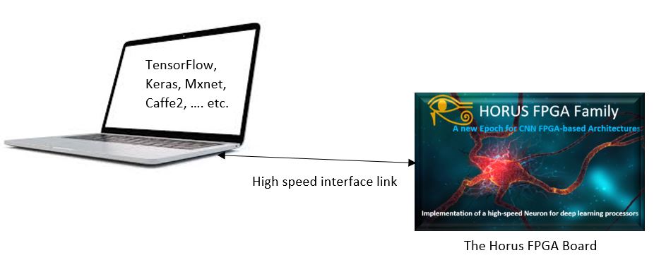
The final stage of this project will be by adding more flexibility to the FPGA architecture to accept any kind of AI models from any software platform (like TensorFlow, Keras, Mxnet, Caffe2, ….etc.) and accelerate the processing of the input data then send the results to the software once again. Also, to add more flexibility to the types of the data that can be received such as Intger16, integer32, or even the smart innovative data types invented by intel such as the FlexPoint. Also, i realized that i need to protoect the idea by apply for patent it.
9. Conclusion
The proposed project and the idea behind it is totally new and can’t be compared even with the innovative solutions provided by intel, Google, or Tesla since I suggest to change the dependence on the fixed architecture platforms that almost created based on the ASIC or GPU chips and to fly to the other flexible horizon, which is to adopt a highly tailored FPGA silicon architecture based hardware platform, that can provide all the advantages that can be gained from the in-the-market product and add to it more important features such flexibility of the interconnection between the innovative sub blocks accelerators embedded in the new suggested FPGA for AI families. Such idea can be achieved so easily and within few months can be in the market by the cooperation between the top leading companies in this field such as intel Altera, Terasic, beside the need to the other important companies such as Analog Devices, ISSI, ... etc. due to the intense need to have high-speed memories in the final product. Also the serial communication need to be replaced by a higher interface protocol as well. Finally, I want to clarify that all what are included here is just the proof-of-concept, demonstrating the main idea, and first-stage prototype of a complex final stage that I’m working on it right now.
1- H. O. Ahmed, M. Ghoneima, and M. Dessouky, "Concurrent MAC Unit Design using VHDL for Deep Learning Networks on FPGA," presented at the IEEE Symposium on Computer Applications & Industrial Electronics (ISCAIE 2018), Penang Island, Malaysia, 2018, Presented and in press.
2- H. O. Ahmed, M. Ghoneima, and M. Dessouky, "2D parallel MAC Unit Hardware Accelerator for Convolutional Neural Network," presented at the Intelligent Systems Conference 2018, London, United Kingdom, 2018, accepted and in Press.
3- H. O. Ahmed, M. Ghoneima, and M. Dessouky, "Pyramidal Neuron Architectures for Accelerating Deep Neural Networks on FPGA," presented at the AHS-2018 : 2018 NASA/ESA Conference on Adaptive Hardware and Systems, Edinburgh, UK, 2018 , accepted and in Press.
4- H. O. Ahmed, M. Ghoneima, and M. Dessouky, "130 nm CMOS Pyramidal Neuron Accelerator for Convolutional Neural Networks," IEEE Transactions on Circuits and Systems I,2018 (Submitted).
5-S. Moini, B. Alizadeh, M. Emad, and R. Ebrahimpour, "A Resource-Limited Hardware Accelerator for Convolutional Neural Networks in Embedded Vision Applications," IEEE Transactions on Circuits and Systems II: Express Briefs, vol. 64, no. 10, pp. 1217 - 1221, 04 April 2017 Oct. 2017.
6- H. Wang, M. Shao, Y. Liu, and W. Zhao, "Enhanced Efficiency 3D Convolution Based on Optimal FPGA Accelerator," IEEE Access vol. 5, pp. 6909 - 6916, 28 April 2017 2017.
7- K. Guo et al., "Angel-Eye: A Complete Design Flow for Mapping CNN Onto Embedded FPGA," IEEE Transactions on Computer-Aided Design of Integrated Circuits and Systems, pp. 35 - 47, 17 May 2017.
8- G. T. Griffin Lacey, Shawki Areibi, "Deep Learning on FPGAs: Past, Present, and Future," 13 Feb 2016.