

EM080 » Hardware acceleration of cryptocurrency for IoT micropayments
In this project we propose to create hardware accelerator for IOTA cryptocurrency transactions. IOTA allows making secure and authenticated quantum resistant channels between IoT devices for communication and micropayments with no fees. Hardware acceleration will allow to reduce transaction time and increase network throughput. FPGA implementation will be flexible enough to adapt for evolving standards, algorithmic methods, or security threats of young IOTA technology. As a result of the project we plan to run hardware accelerated IOTA node on Intel FPGA DE10-Nano board.
The core of IOTA is called Tangle and unlike Blockchain has Directed Acyclic Graph structure. There are no miners in the Tangle and IoT devices themselves maintain network operation, which leads to unlimited scalability and absence of fees.
For adding new transactions to the Tangle, IoT devices need to perform some Proof-of-Work (POW) for spam and Sybil attack protection — iteratively calculate Curl hash function for the transaction and change nonce field of the transaction until obtained result doesn’t satisfy given criteria. Curl is new quantum resistant hash function created by IOTA team. The software implementation of Curl on embedded platforms is very slow so hardware acceleration of Curl and POW operations are relevant tasks.
The target audience of the proposed hardware accelerator is very large. It is literally any Intel FPGA based IoT device that will use IOTA features of secured messaging and micropayments with no fees. Broadly, in case of silicon implementation of the proposed accelerator, the target can be almost any IoT device.
To run hardware accelerated IOTA node on Intel FPGA platform it is necessary to perform the following tasks:
create hardware implementation of Curl & POW accelerators in Verilog;
verify Curl & POW hardware accelerators using System Verilog and UVM;
synthesize Curl & POW hardware accelerators for Cyclone V FPGA and integrate it into ARM based System-on-Chip;
develop Linux drivers for Curl & POW hardware accelerators;
port IOTA light node to DE10-Nano and replace Curl & POW software implementation by driver call to hardware;
High level block diagram for the proposed system
Hardware acceleration of Curl hash function will allow to reduce transaction time and increase IOTA network throughput, boosting performance of the system.
The great benefit of Intel FPGA platform is HPS system on the same crystal with FPGA. This allow implement IoT applications without external microcomputer, utilizing Intel FPGA embedded ARM & Linux. The high speed 256 bit bus between HPS and FPGA will significantly increase throughput of data transfer to/from hardware accelerator. HPS F2H SDRAM interface will allow make DMA transactions with DDR3 memory freeing ARM processor from data copying work.
FPGA implementation will guarantee rapid adaptation to changes. Now IOTA is at early stage of development, so such an approach will be flexible enough to easy make all subsequent modifications related to evolving standards, algorithmic methods, or security threats, that is ideal for prototyping.
E.g. some time ago researchers from MIT found vulnerability in Curl hash [1]. Although real IOTA network was not hacked exploiting this vulnerability, IOTA developers as a precaution decided use Keccak for signing transactions instead of Curl. Now Curl is still used in IOTA for the POW operation and best cryptographers works on Curl improvment. After releasing new version of a Curl, FPGA implementation can be easily adopted to such changes, compared to pure silicon implementation.
And last, but not least, running IOTA node on Intel FPGA will allow easily integrate new sensors and interfaces, expanding I/O capabilities of IoT system.
Secured messaging is a critical feature for the IoT devices. IOTA technology introduces so called Masked Authenticated Messages (MaM). With MAM your IoT devices will have an ability of messaging in publish/subscribe decentralized manner with highest level of security and integrity [2]. Another killer feature of IOTA is micropayments with no fees which will allow sell your sensor data with lowest price and still be in profit!
To benefit from IOTA features you should be able to send IOTA transations. The rate of IOTA transactions limited by POW operation. Due to slow calculation of software implemented Curl, the POW operation on embedded devices can last up to 50 minutes!
The goal of our project is to speedup sending IOTA transactions by creating hardware accelerators for Curl & POW operations.
Proposed accelerators could be used on any IoT device that will utilize IOTA features.
This project was implemented by 2 people: Ievgen Korotkyi (associate professor) and Serhii Sachov (master student) from Open Hardware Laboratory Lampa (Igor Sikorsky Kyiv Polytechnic Institute, Department of Design of Electronic Digital Equipment). We created Curl & POW hardware accelerators (and high level SV models), integrated these accelerators into ARM based SoCs, developed Linux drivers for each accelerator and SV/UVM verification testbench, performed integration into IOTA light node (written in Go Lang).
The duration of project implementation was 3 month (feb-april 2018). Before the beginning we had no experience with IOTA and hardware implementation of POW and hash functions.
We started this project completely from scratch. The main sources of information about IOTA, Curl and POW were source codes on IOTA github [3] and youtube tutorials like [4].
Before we dive into details of proposed hardware accelerators, let's examine the basic concepts: ternary numeral system, Curl hash algorithm and IOTA POW operation.
5.1. Ternary numeral system
To be secured from quantum computer attacks IOTA introduced ternary hash function Curl that operates in ternary numeral system. The numbers in ternary system consists of trits. Each trit can take a value of -1, 0, 1. Three trits form a tryte. Each tryte has 3^3=27 combinations. For trytes representation IOTA uses capital letters A-Z and number 9. It is IOTA tryte alphabet. More information about IOTA trits and trytes you can find in [4].
In our project for trit representation in digital FPGA devices we use 2 bit numbers with one forbidden combination 2'b10.
5.2. Curl hash algorithm
As mentioned above, we studied Curl algorithm by analysing source codes from IOTA github. E.g. CCURL library which is implementation of Curl algorithm in C [5].
To calculate a hash from input data Curl utilize Sponge Construction. The first stage of Sponge Construction is Absorbing input data into state variable of fixed length. The next step is Squeezing hash of given length from the state. The main operation used in Absorb and Squeeze stages is Transform.
The block diagrams for Absorb, Squeeze and Transform algorithms utilized in Curl represented on Figures 1-3 respectively.
The length of Curl state is 729 trits (1458 bits in binary implementation). During Absorb and Squeeze operations, input/output data loaded to/from low 243 trits of the state. Transform operates on the whole state. There are 81 rounds of state permutations during Transform.
 Figure 3. Block diagram for Curl Transform operation
![]()
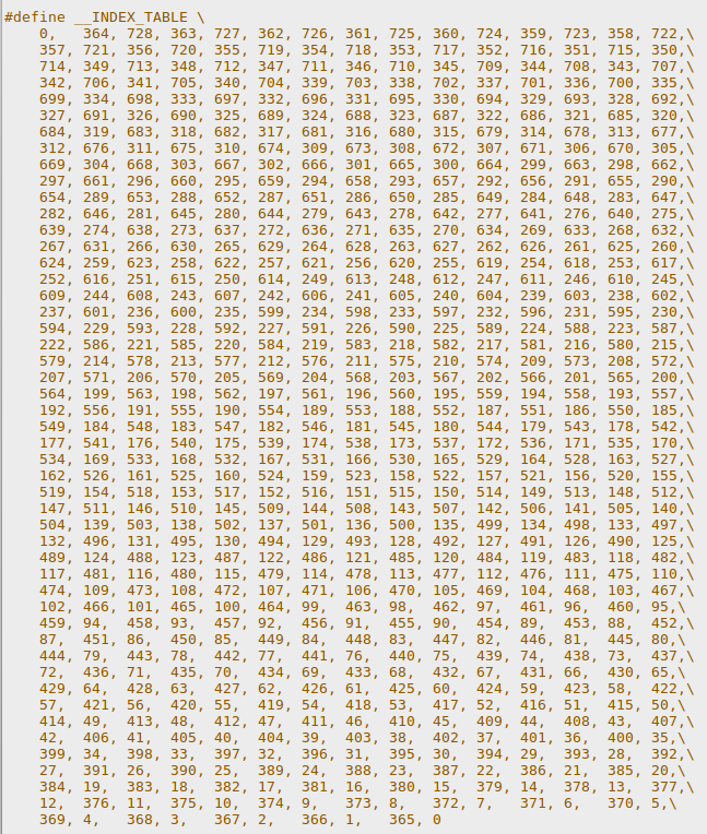
The index table used in Transform operation (starting from 0 index) listed on Figure 4.
Figure 4. Index Table for Transform operation
The TRUTH_TABLE is very simple:
signed_byte_t [0:8] TRUTH_TABLE = '{1, 0, -1, 1, -1, 0, -1, 1, 0};
5.3. IOTA POW operation
Before sending new transaction to the Tangle, IoT devices need to perform POW operation on the transaction, otherwise this transaction would be rejected by the Tangle.
The POW operation is iterative calculation of Curl hash of the transaction and changing nonce field of the transaction until obtained result doesn’t satisfy given criteria. This criteria is some amount of zero trits at the end of obtained Curl hash. Required amount of zeros called Minimum Weight Magnitude (MWM) and for now this value is 15.
The nonce field consists of last 27 trytes (81 trits) of the IOTA transaction. The structure of IOTA transaction can be found in [6]. At the end of the POW operation, nonce should containt any valid ternary value for which last MWM trits in Curl hash from IOTA transaction will have zero values. As you can guess there can be several valid nonce values for given transaction. Some software POW implementaions starting from zero nonce and then iteratively increment it. In our device we use random generation of a nonce with the aid of LFSR for increasing maximum clock rate (combinational ternary incrementer takes a lot of resources and has long delay).
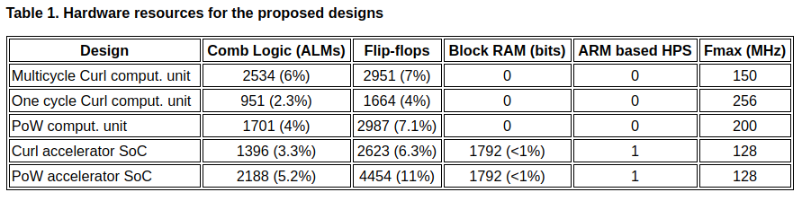
In this section we'll describe performance of the proposed accelerators and hardware resources needed for it implementation.
The hardware resources for all proposed designs summarized in Table 1. The target FPGA device is 5CSEBA6U23I7 installed on DE10-nano board.
The largest design is a SoC for solving POW task. It utilizes 11% of target FPGA.
We optimized Curl & POW computational units for maximum clock frequency: 256 MHz for Curl comput. unit and 200 MHz for POW comput. unit. Unfortunately we had no time for optimisation of the SoCs for these calculation units. So the maximum clock rate for Curl & POW SoCs is 128 MHs. We think that clock rate for these SoCs can be significantly improved. It will be the task for future work.
During measuring performance parameters we launched target systems on 100 MHz clock rate.
First we compiled CCURL library [5] from IOTA developers for DE10-nano embedded Linux. CCURL includes tools for Curl calculation, POW operation and trytes-to-trits/trits-to-trytes conversion.
Then we wrote simple programs for measuring hash rates of software and hardware Curl implementations. During given period of time (which is argument of a program) we measured pure Curl calculation time and counted the number of calculated hashes. At the end we divided hash count by work time to obtain hashrate.
We measured Curl calculation time as follows. At the beginig of calculation we saved current time in ms obtained from gettimeofday() Linux API. Then we performed calculation and at the end of calculation again measured current time in ms and subtract obtained values. For software calculation of the Curl we used absorb() and squeeze() methods from CCURL library.
The source code for measuring hash rate of software Curl implementation can be found here. The source code for measuring hash rate of hardware Curl implementation can be found there.
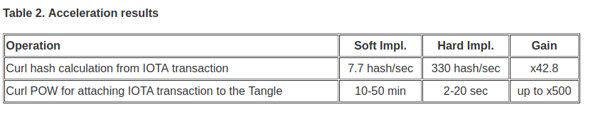
The speedup for proposed hardware Curl accelerator compared to CCURL software implementation was x42.8. More details about obtained hashrates you can find in Table 2.
To measure performance of a POW operation we took raw IOTA transaction from the Tangle, following the instructions from [9] and change it nonce. Then we tried to solve POW task with CCURL software implementation for MWM=15. It took 52 minutes on DE10-nano board. It is unacceptably long time! Proposed Curl hardware accelerator solved POW task for the same transaction and MWM in 6 seconds with x500 speedup.
For other IOTA transactions the average time for software POW calculation was nearly 10-20 minutes. It is still very long time. The duration of hardware accelerated Curl computation varied from 2 to 20 seconds.
In final experiment we sent two messages to IOTA Tangle utilizing GIOTA [7] and GMAM [8] libs written by IOTA team in Go Lang and compiled for DE10-nano board. It takes 8 min 38 sec to send a message with software POW. With hardware accelerator, integrated into GIOTA lib, the message was sent in 5.5 sec with x90 speedup. You can explore these messages in the Tangle.
Acceleration results summarized in Table 2. You can watch all mentioned experiments in design video.
 Curl POW Hashrate for hardware accelerator: 1 204 819 hash/sec
UPDATE 1
After 30th of April we significantly improved design and make it parameterizable. One can manually set the number of POW computing units by changing parameter value.
Performance & Resources for new parameterized design:
Proof-of-Concept implementation for DE10-nano board has following parameters:
It looks like for DE10-nano is possible to increase the number of POW computing units up to 20 and obtain 25 Mhash/sec on 100 MHz, but we do not have enough RAM on our laptops to synthesize such large system.
UPDATE 2
We discovered that other teams continuously improve their projects in the first half of July. So we decided to increase performance of our design :)
To do these, during 12-14 JUL we bought additional RAM and instantiated more POW accelerators. To improve scalability we introduce parameters CL_NUM and CU_NUM. Parameter CL_NUM specifies the number of POW clusters. Parameter CU_NUM defines the number of POW computing units per cluster.
In previous release we used one POW cluster with 11 POW computing units. But increasing the number of POW computing units inside one POW cluster has bad scalability (high connectivity between midstate reg and state regs of POW computing units inside one cluster introduces routing congestion). Much more better is to increase the number of POW clusters with reasonable number of POW computing units inside each one (4-5 POW computing units per POW cluster).
Our final Proof-of-Concept implementation:
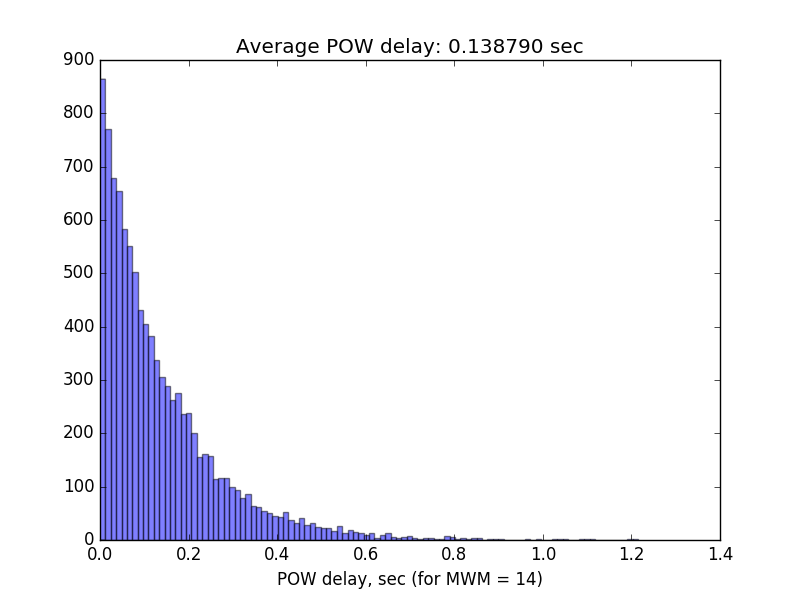
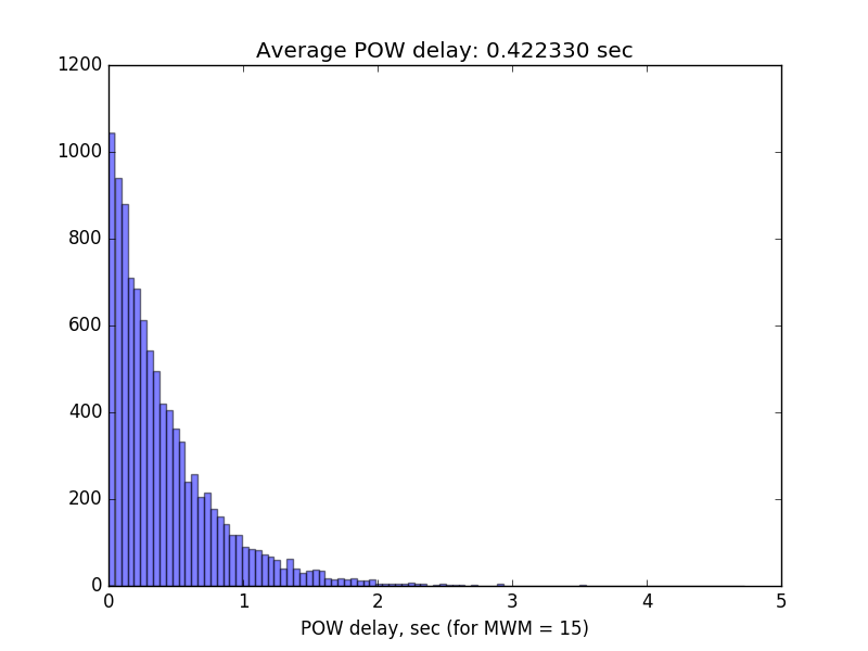
We created several histograms for the PoW-time of 10 000 randomly generated IOTA transactions.
On our github you can find source code for this performance testing tool.
Here the histogram for POW delays in case of MWM = 14. As you can observe, almost all delays are within 0.6 sec with average of 0.14 sec. Measurement time for all 10 000 transactions was 24 minutes.
The following picture represents POW delays for MWM = 15. Almost all delays are within 2 sec with average of 0.42 sec. Measurements for 10 000 transactions were completed in 71 minutes.
To the best of our knowledge, we created fastest IOTA POW accelerator in the world for embedded applications (as of 15 July 2018).
Anyone can check the presented results by analyzing source code of our project on github.
Also you can download Linux sd-card image for IOTA hardware accelerator on DE10-nano board and the latest rbf file.
7.1. High level System Verilog implementation of Curl lib
We started work on this project from porting CCURL library to high level Sytem Verilog. We created SV implementation for absorb, squeeze, transform, trytes-to-trits and trits-to-trytes functions. Then we verified obtained results against reference CCURL implementation with the aid of DPI.
This was very useful for understanding the operation principle of Curl algorithm. This Curl SV lib can be used for verification of Curl based digital designs in case when one have no DPI license.
The source code for high level Curl library in System Verilog can be found here.
7.2. Simple multicycle Curl calculation unit
Our first Curl hardware accelerator implemented transform function from Figure 3 in sequential multicycle fashion. The structure of this solution depicted on Figure 5.
For each round this design needs 729 cycles to calculate new state. For 81 Curl rounds, to transform each 243 trit data block we need 729*81=59049 cycles. IOTA transaction contains 33 such data blocks. So to compute hash from IOTA transaction with this implementation we need 1948617 cycles. The hardware resources for this design can be find in Table 1.
Obviously this design is inefficient but at the begining of the work we had no ideas how to implement Curl transform better. Source code for simple multicycle implementation.
Figure 5. Architecture of simple multicycle Curl calculation unit

7.3. One cycle Curl calculation unit
After some brainstorming we realized that each trit of new state depends from two prev. state trits in predictable manner (you can check this by analyzing index table from Figure 4):
new_state[0] <- state[0], state[364]
new_state[1] <- state[364], state[728]
new_state[2] <- state[728], state[363]
new_state[3] <- state[363], state[727]
new_state[4] <- state[727], state[362]
new_state[5] <- state[362], state[726]
and so on ...
This observation allow build one cycle Curl transform unit with structure presented on Figure 6. The logic for generating new Curl state from prev. state in one cycle shown on Figure 7.
Figure 6. Architecture of one cycle Curl calculation unit

Figure 7. Logic for generating new Curl state from prev. state in one cycle
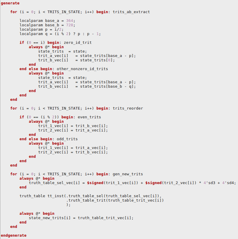
This implementation calculates each Curl round in single cycle. For the whole transform operation it needs 81 cycles. Curl hash from IOTA transaction (composed of 33 243-trit data blocks) calculated for 33*81=2673 cycles.
We optimized this one cycle implementation by maximum clock rate, so Fmax is 256 MHz.
Hardware resources needed for implementation are: 951 ALM, 1664 flip-flops.
Source code for optimized one cycle implementation of Curl hardware computation unit.
7.4. POW hardware calculation unit
Proposed POW hardware calculation unit based on our one cycle Curl computation unit. Because the nonce fileld is the last 81 trits of the transaction, first we should absorb all previous trits into the state register. Then we save the state into midstate register and starting search for a valid nonce.
At the begining of each iteration we load state from midstate, change nonce, calculate Curl transform for this state and check last MWM trits for zero value. And doing this until find the valid nonce for which the last MWM trits of Curl transform are zeroes.
The tricky part here is finding new values for the nonce. We realized that combinational ternary incrementer takes a lot of hardware resources and has long delay. So we decided randomly generate new trits for the nonce via LFSR. But it is important to check each new trit obtained from LFSR for forbidden value 2'b10 and in such a case return some valid value (e.g. 2'b00 or 2'b11).
The hardware resources for implementation of proposed POW hardware calculation unit are: 1701 ALM, 2987 FF.
Maximum clock frequency is 200 MHz.
Source code for POW hardware calculation unit
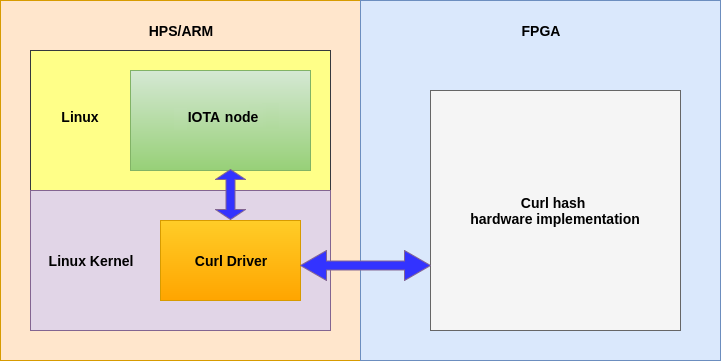
7.5. SoC for Curl and POW hardware accelerators
We created two Systems-on-Chip: one for Curl hardware accelerator and one for IOTA POW accelerator. Hardware resources for both SoCs you can find in Table 1.
The structure of the both SoCs is the same with minor differences. Globally these SoCs are differ only in type of computational unit (Curl/POW accelerator). The architecture of proposed SoCs presented on Figure 8.
Figure 8. HW/SW architecture of IOTA hardware accelerator
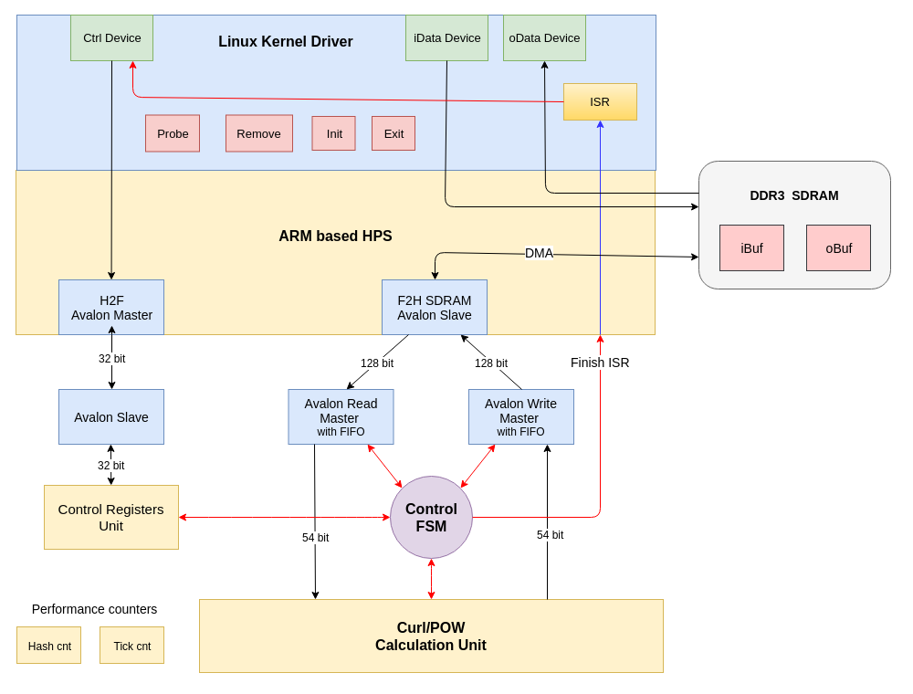
Each SoC has two Avalon interfaces: 32 bit slave interface and 128 bit master insterface.
Via Avalon slave interface ARM can read/write accelerator's control registers.
Register map for Curl accelerator:
REG 0: main ctrl reg (bit0:finish, bit1:start, bit8-23:src_buf_len in trits)
REG 1: src buf addr in SDRAM (addr in 128 bit words)
REG 2: dst buf addr in SDRAM (addr in 128 bit words)
Register map for POW accelerator:
REG 0: main ctrl reg (bit0:finish, bit1:start)
REG 1: src buf addr (addr in 128 bit words)
REG 2: dst buf addr (addr in 128 bit words)
REG 3: mask for mwm
REG 4: hash_cnt reg
REG 5: tick_cnt low reg
REG 6: tick_cnt hi reg
POW accelerator SoC counting duration of POW operation in clock cycles and the number of evaluated hashes. This info can be read by driver and used for calculation of hashrate.
Avalon master connected to F2H SDRAM Slave interface of HPS and through this interface our accelerator can perform read/write DMA transactions with SDRAM memory (e.g. read input transations from input buffer and write calculated hashes to destination buffer in SDRAM). In this project we reused instances of Avalon Read/Write masters from [10].
After ARM set addresses of src and dst buffers and triggered start bit in main control register via slave interface, control FSM goes to LOAD state and launch Avalon read master. Avalon read master starts to read input data from src buffer in SDRAM. Control FSM loads data from Avalon read master to curl/pow calculation unit and periodically starting transform operation (and going to TRANSFORM state during the period of transform) until all input trits will be processed in a case of Curl accelerator. In a case of POW accelerator Control FSM goes to POW state and generate strobe for starting POW. After the end of calculation, Control FSM goes to STORE state and store calculation result from computaion unit to dst buffer in SDRAM via Avalon write master. After finishing all operations Control FSM generates interrupt to HPS and goes to IDLE state.
UPDATE
After 30th of April we significantly improved design and make it parameterizable. It is possible manually set the number of POW computing units by changing parameter value.
In such parameterizable system one POW computing unit is master and all remaining are slaves. Master POW unit absorbs all trits from IOTA transaction, except nonce part, to midstate register. Then all POW computing units (master and slaves) preload own state registers from midstate, randomly change personal nonces and starts iterative search of valid nonce. When one of POW computing units finds a valid nonce, POW operation ends, control FSM stores nonce to destination bufer in SDRAM and generates finish interrupt for ARM CPU.
7.6. Linux driver
To simplify communication between user space programs and hardware accelerator we developed drivers for Curl and POW hardware accelerators. During these drivers creation, instructions from [12] and [13] were very helpful.
In Probe function each driver allocates source and destination DMA buffers and sends adresses of these buffers to accelarator control registers (actually we should send addresses divided by 16 because we need addresses in 128 bit words). Also in probe function we register callback for the interrupt and create three devices: control device, input data device, output data device.
We can write data to src DMA buffer in Linux kernel via fwrite file operation of input data device. We also can read dst buffer with fread operation of output data device. By writing data with fwrite to control device we can send some control information to driver (input transaction length or MWM). Reading from control device launches calculation (for Curl hash or POW depending on used SoC/driver). On the begining of control device read proc, driver set accelerator's start bit (launches computations) and go to sleep. When accelerator finish computations, it generates interrupt. Interrupt callback simply wakeup blocked control fread func from sleep and fread returns control to user space program. After this user space program can read calculated result from output data device.
Source code for Curl accelerator's driver
Source code for IOTA POW accelerator's driver
7.7. Compiling Linux Kernel and rootfs
For this project we compiled Linux Kernel ver. 4.9.78-ltsi with the help of instructions from [13] and [14]. Also we built Debian rootfs utilizing debootstrap following instructions from [15]. The contents of /lib/modules we took from Angstrom compiled with instructions from [16]. Debian distribution has excellent packet manager which allows to build and install all other necessary things.
7.8. Integration with IOTA
In order to integrate our POW hardware accelerator with IOTA, we modified source code of gIOTA [7], which is a light node client written in GoLang.
Before launching POW operation gIOTA searches a most suitable POW function for the target platform (method GetBestPoW() in file pow_go.go). At the beginning of GetBestPoW() we simply checking presence of hardware accelerator's driver (/dev/cpow-ctrl device) and if it exists, we return PowFPGA() function. For other platforms or in case of unloaded driver GetBestPoW() will return POW function implemented in C.
The source code for PowFPGA() function one can find here. We convert transaction from trytes to trits, allocate memory for the nonce and make a call to pworkFPGA() written in C language. Method pworkFPGA() writes transaction to the input buffer of accelerator's driver (/dev/cpow-idata device), launces POW operation by reading from driver's control device (/dev/cpow-ctrl device) and finally reads calculated nonce from output buffer of the driver (dev/cpow-odata device). At the end of PowFPGA() function we return trytes for calculated nonce.
For sending messages to IOTA Tangle in our video demo we used standard messaging client [8]. The source code for sending messages one can find there.
7.9. UVM testbench
Created Curl hardware accelerator was verified with UVM testbench (source code). Our UVM testbench contains the next blocks:
Avalon S/M interfaces;
Avalon S/M active agents;
Avalon S/M passive agents;
Collector of input and output data;
Synchronization monitor;
Reference model of Curl hash algorithm;
Scoreboard;
Sequences;
All this blocks are shown on Figure 9.
Figure 9. Architecture of UVM design testbench
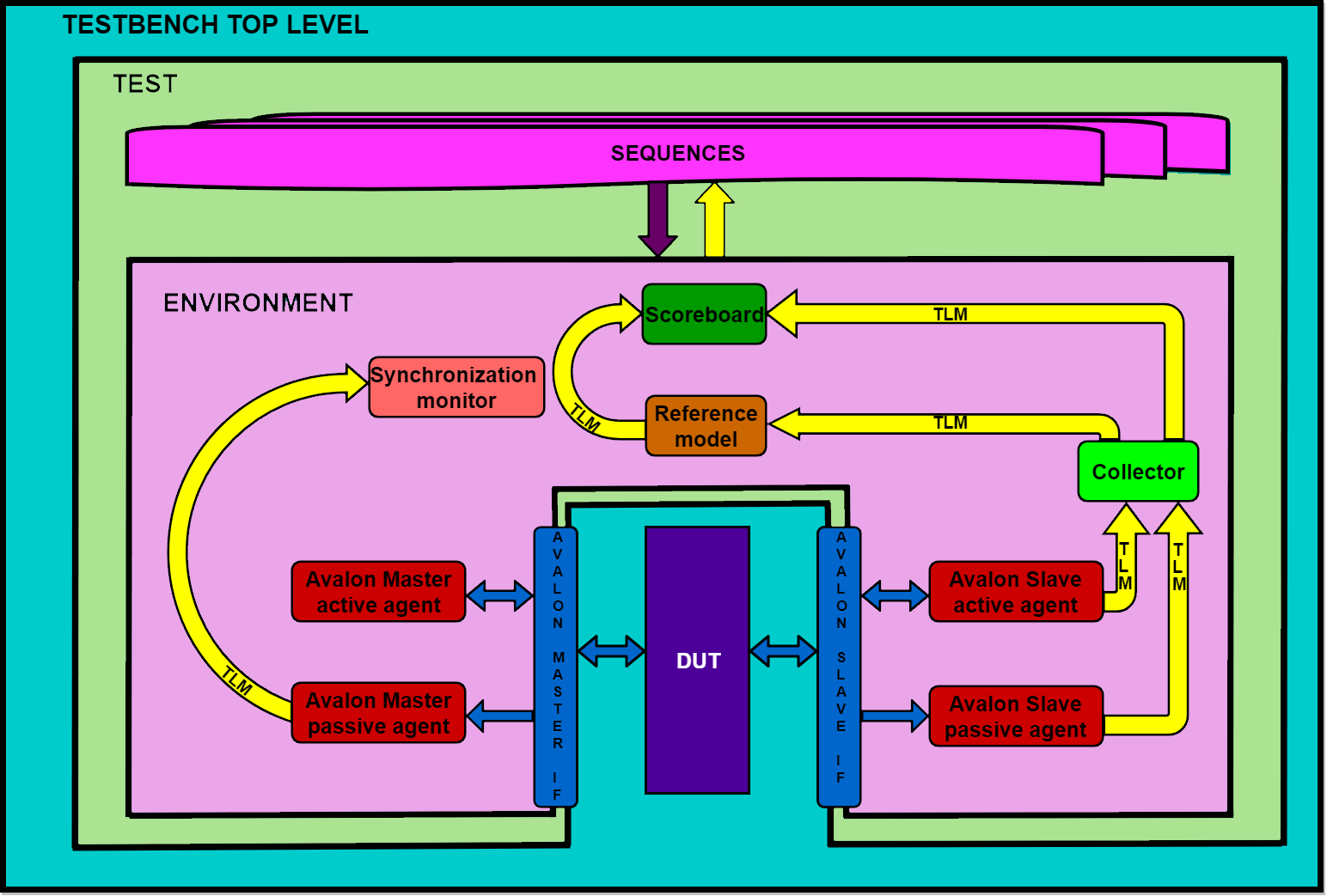
Avalon M active agent, shown on Figure 10, simulates CPU. Driver sends stimulus to Avalon M interface which contains source address of input transaction, output address for storing calculated hash, length of input transaction and a start bit for DUT (Design Under Test) control registers. Sequencer takes this stimulus from sequences and sends to driver. Also driver reads value of control registers, for example, status register. Active monitor records stimulus from Avalon M interface, which were made by driver. Active monitor can send this stimulus to another block, which have to be connected with monitor via TLM (Transaction Level Modeling). In our architecture this Active monitor is not used.
Figure 10. Architecture of Avalon active&passive agents

Avalon M passive monitor takes stimulus from Avalon M interface, which were made by DUT and sends this data to synchronization monitor via TLM.
Avalon S active agent, shown on Figure 10, simulates RAM. The driver of this agent contains an array (representing memory) where it stored input transactions which sequencer obtained from sequences and send to driver. Active monitor takes input transaction (which DUT reads from RAM) from Avalon S interface and sends it to the collector via TLM.
Avalon S passive monitor takes output data from DUT via Avalon S interface, and sends it to collector via TLM.
Avalon M/S interfaces and Avalon M/S drivers were written using parts from Avalon-MM Interface Verification IP [11].
In build phase active agents creates drivers, sequencers and active monitors using factory. In connect phase agents connects drivers with their sequencers via TLM.
In build phase passive agents creates a passive monitors using factory.
Synchronization monitor takes data from Avalon M passive monitor and check an information about DUT calculation. If DUT finish hash calculation, this monitor sends a command to sequences about enabling of next test.
Collector collects parts of input transaction from Avalon S active monitor into full transaction and sends it to reference model via TLM. Also collector collects parts of output hash result from Avalon S passive monitor and sends it to scoreboard via TLM.
Reference model was taken from CCurl library, written by IOTA team, and integrated to testbench via DPI. Every time, when collector sends input transaction, C Curl hash algorithm makes a calculation of hash function and after that sends the result to scoreboard via TLM.
Scoreboard compares an output result from DUT with output result from reference model and generates an information about comparison result.
Environment includes all objects, that were described above. In build phase environment build all active and passive agents, collector, synchronization monitor and scoreboard using factory. In connect phase of simulation this object makes all connections via TLM.
Sequences consists of sequences for Avalon S/M drivers for start and final initialization of this drivers, commands with input information for Avalon M driver and commands with input transaction, that randomly generated in trytes and converted into trits, for Avalon S driver.
Test includes environment and top sequence. In build phase test creates an environment using factory. In run phase test connects sequencers from environment with sequencer in sequences. After performing all sequences run phase preparing to finish.
Top level of testbench connects DUT with Test, generates input clock and reset signals and start the test.
Design was verified via 500 tests and all of that was successful!
8. Conclusion
In this project we created hardware accelerators for Curl hash and IOTA POW operations. The proof-of-concept implementations were launched on DE10-nano board.
Compared to reference CCURL library our hardware accelerator demonstrates x42.8 speedup during calculation of Curl hashes. The speedup for POW operation is x90 ÷ x500 times compared to CCURL and GIOTA reference software implementations on DE10-nano board.
For all proposed designs hardware resources needed for implementation are no more then 11% of 5CSEBA6U23I7 FPGA device.
The hashrate obtained during POW is 1 204 819 hash/sec.
In future we plan to increase clock frequency and utilize several POW accelerators working in parallel to achieve 10 Mhash/sec.
UPDATE 1
After 30th of April we significantly improved design. Final implementation of IOTA POW hardware accelerator for DE10-nano contains 11 POW computing units, delivers 13.2 MH/s and x1000 speedup (compared to software implementation from IOTA developers) for only 30% of FPGA resources.
In future we plan to unroll 81 rounds of transform-function into pipeline and feed midstate with new nonce in this pipeline on each clock cycle. This will significantly increase performance of POW calculation. Also we want to add PCIe interface to such system and synthesize this system for board with huge FPGA and PCIe (e.g. DE5-Net). It can be great hardware accelerator for IOTA full nodes in cloud data centers.
UPDATE 2
Our final Proof-of-Concept implementation:
To the best of our knowledge, we created fastest IOTA POW accelerator in the world for embedded applications (as of 15 July 2018).
9. References
2. IOTA: MAM Eloquently Explained
3. IOTA source codes on github
4. IOTA tutorial: Trit and Tryte
5. CCURL - C port of Curl library from IOTA team
6. Structure of IOTA transaction
7. gIOTA: The IOTA Go API Library
8. IOTA messaging client in Go Lang
9. IOTA tutorial: Proof of Work, Curl and Nonce
10. Avalon Memory-Mapped Master Templates
11. Avalon-MM Interface Verification IP
12. Developing Drivers for Altera SoC
13. BUILDING EMBEDDED LINUX FOR THE TERASIC DE10-NANO (AND OTHER CYCLONE V SOC FPGAS)
14. Embedded Linux Beginners Guide