

PR069 » Information Encryption for Internet of Things Device
At present, IoT devices are in an explosive growth stage. According to IDC statistics, the total investment in the global IoT market in 2016 was 736.9 billion U.S. dollars, and by 2020 this figure will reach 1.2899 trillion U.S. dollars. However, the security issues of IoT devices are also getting worse day by day and there are many devices are vulnerable to security breaches. For example, at the end of 2016, Mirai malware infected a large number of IoT devices and formed a botnet to launch a DDoS attack on the world famous DNS provider Dyn, resulting in the failure of PayPal websites to pay and social websites such as Twitter and Tumblr can not log in. Therefore, the problem of information security can not be effectively solved, which will seriously hinder the popularization and application of Internet equipment. In response to the above problems, this product relies on the FPGA platform to design a SOC (system on chip) that supports multiple cryptographic modules such as the National Security Algorithm SM2 / SM3 / SM4, the International Cryptographic Algorithm AES and the Physical Unclonable Function (PUF) To ensure the information security of IoT devices.
Summary:
At present,the Internet of Things(IoT) is widely used in many fileds involved intelligent transportation, environmental protection, government work, public safety, safe home, intelligent fire control, industrial monitoring, environmental monitoring,which make our lives more convenient.
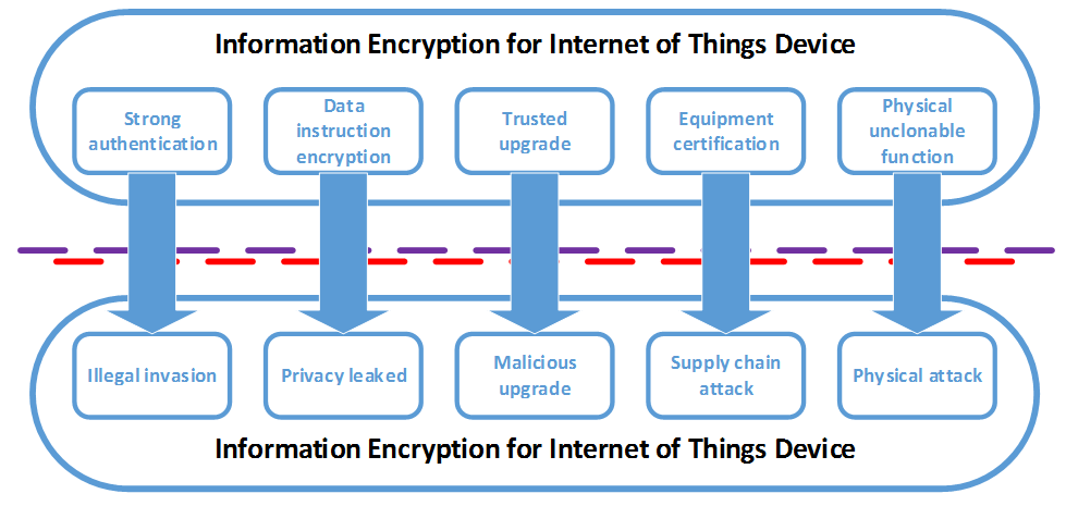
But at the same time,there are still some flaws in the product information security of the Internet of Things: weak authentication mechanism, Web application vulnerabilities, leakage of user privacy, and unsigned firmware update, which make it easy for attackers to compromise the system network, crack passwords for IoT devices, and even completely control the device through malicious firmware updates.
In response to the above problems,this paper proposes a system with a DE10-nano FPGA board to ensure the Internet of Things device information security ,using SM4 block cipher algorithm.In this system we design a physically unclonable function (PUF) as the key generator making the process of encryption safer. Specific product features as shown below:
Innovations:
⑴、PUF,a physically unclonable function,which means that we give an input of a stimulus to a physical entity and it will output an unpredictable response using a random difference in its inevitable internal physical construction.
Because of some useful features of PUF, generate keys with PUF has following advantage:
①The anti-tampering feature of PUF can be used to provide tamper-resistant key storage.
②A key generated by PUF is closely related to the physical harware embeddedin the PUF,making the entire hardware physically unclonable.
③A PUF with a fuzzt extraction module is more efficient than a non-volatile storage unit in securely store an encryption key.
④Since the randomness of the digital circuit of key generator is caused by unavoidable manufacturing difference,the process of explicit key programing is not required,which simplifies key distribution.
⑵、Innovative use of SM4,which was issued by the National Cryptography Administration in 2012.The SM4 cryptographic algorithm has been fully analyzed and tested by professional cryptographic institutions in China and can resist existing attacks such as differential attacks and linear attacks.
⑶、The use of FPGA's powerful parallel processing capabilities to achieve a variety of hardware acceleration algorithm.
⑷、Utilize ARM processor and FPGA programmable logic structure to realize software and hardware cutting and improve system flexibility.
System scheme
At present, many symmetric encryption algorithms such as AES and SM4 store keys in nonvolatile memories such as Flash. Attackers can steal or tamper with keys by invasive attacks. The PUF's response will only be output when it is powered on, and will automatically disappear when the power is turned off. Because the PUF response doesn’t need to save and has random and unpredictable characteristics. Therefore, using the PUF response as a key can effectively prevent intrusive attacks and prevent keys from being copied or stolen. The tamper-resistant properties of the PUF can provide tamper-proof key storage without the need for traditional non-volatile storage steps, thus ensuring the security and reliability of the system key. Then based on a secure and reliable key, we use the SM4 algorithm to encrypt the data. SM4 algorithm is a grouping algorithm, its algorithm is simple and its structure is safe and efficient. The data packet is 128 bits in length and the key length is 128 bits. Both the encryption algorithm and the key expansion algorithm take 32 rounds of iterative structure. The SM4 cipher algorithm is a pairwise operation, so the structure of the decryption algorithm is the same as that of the encryption algorithm, except that the order of use of the round keys is reversed, and the decryption round key is the reverse of the encryption round key. SM4 is currently a great encryption and decryption algorithm, so this program uses this encryption and decryption scheme.
I、Physical Map
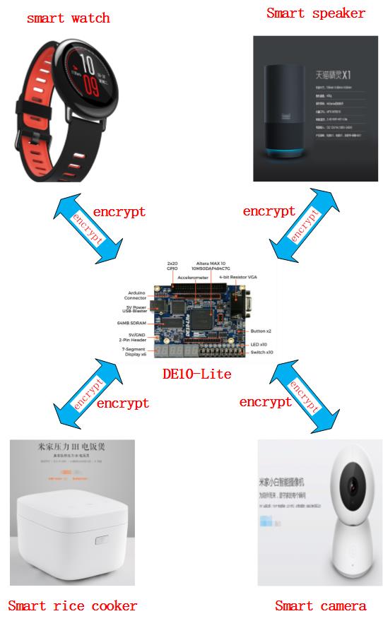
Fig 1 . Physical map
II、Working Diagram
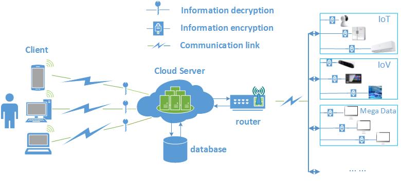
Fig 2 . Working diagram
III、Digital Hardware Architecture
This design includes a central processor interconnected by an on-chip bus, dynamic memory, SM2 encryption algorithm unit, SM3 encryption algorithm unit, SM4 encryption algorithm unit, AES encryption algorithm unit, physical unclonable function circuit, I2C interface, UART interface, SPI interface , I / O port, JTAG interface, WIFI interface, timer and PLL. The design encryption and decryption operation faster, with less hardware resource consumption and lower power consumption, the key can not be copied and theft, security, security level higher. Specific digital hardware structure shown in Figure 3.
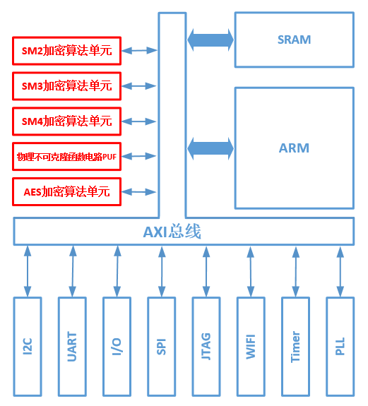
Fig 3 . Digital Hardware architecture
IV、Work Flow Chart
In this design, through the research and analysis of the computational complexity and development cycle of the system, we design a hardware and software partitioning way and the method of implementing secure communication under the premise of meeting the low power consumption and the area of the product. The design can reduce the execution time of the algorithm module itself and reduce the number of times the module is invoked during the algorithm implementation. Compared with the hardware implementation, multiple register resources can be saved and it is more flexible and convenient to modify the algorithm. The process can only be public-key signature with 64-byte . The design can effectively reduce the chip area and improve system operation efficiency and performance. Work flow chart shown in Figure 4.
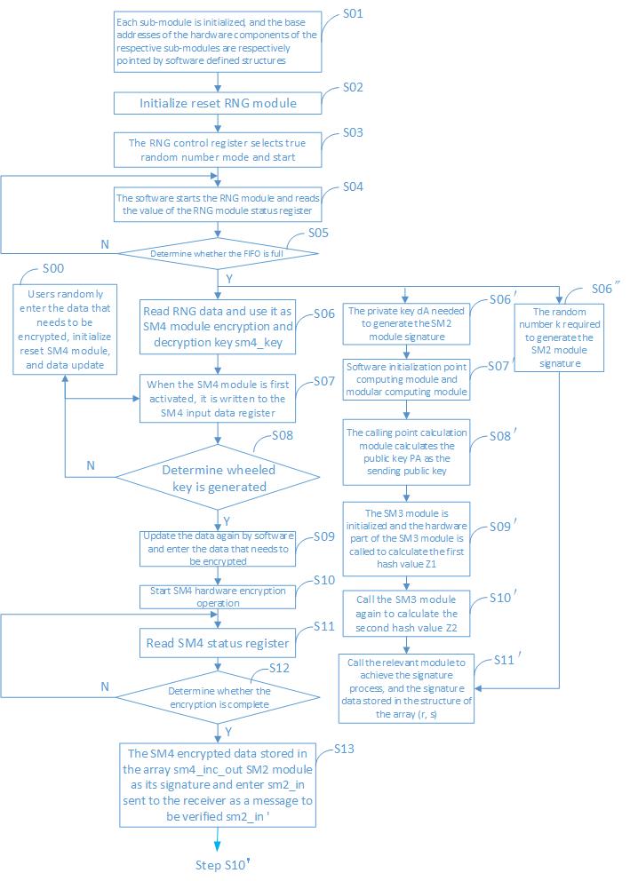
Fig 4 . work flow chart
⑴Hardware
There are both FPGA logic and NiosII processor on the SoC FPGA chip. And the resources on DE10-Nano SoC FPGA Kit are following:
①On FPGA side
5CSEBA6U23I7 device (110K LEs)
EPCS64 Serial configuration device
HDMI TX compatible with DVI 1.0 and HDCP v1.4
②On HPS side
100MHz Dual-core ARM Cortex-A9 processor
1GB DDR3 SDRAM (32-bit data bus)
1 Gigabit Ethernet PHY with RJ45 connector
Micro SD card socket
UART to USB, USB Mini-B connector
③Avalon-Bridge
On SoC FPGA there is Avalon-Bridges to make the communication between FPGA and NiosII much more convenient and faster.
⑵Conclusion
This design is based on FPGA development, the following two points is Intel's FPGA in the design of the main role:
①FPGA parallel computing power IoT devices work will produce a lot of real-time data, which requires our design to have a very strong high-speed processing capabilities. When dealing with large data streams, the primary advantage of FPGAs compared to microprocessors is the ability to perform logical operations and assignments on a large number of variables at the same time, enabling parallel operations and improving the data processing capabilities of the product.
②the internal integrated NiosII processor. In the design of some of the functions if the way through the hardware design to achieve, then the design process will consume more resources, this design is a bit outweigh the benefits. In this case, the DE10 integrated with the NiosII processor can provide a good solution. Through proper software and hardware partitioning, the system function design by the NiosII and the FPGA in coordination will achieve a multiplier effect.
The purpose of this design has been introduced in the "High-level Project Description" section. The main design goal is as shown in the title, so no more introduction in this section. We will introduce the problems encountered in the design process and solutions:
⑴ We combine HPS to Build a Hardware Environment after completed the design of custom IP for PUF and SM4. And then we want to Cross-compilate between hardware and software. But the linux system will always restart automatically and reload the preloaded hardware of the DE10 board in the experiment. In this issue, we have communicated with Terasic's artisan of technical support several times and failed to resolve finnally. In order to be able to submit the work before 30th april, we chose to use the NiosII processor and switch the AXI bus to the Avalon bus. Due to this change, the operating frequency of the design and the transmission capability of the bus are affected. So if who can solve this problem, you can express your own suggestion at the bottom of the proposal. we be greatly appreciated.
⑵ Due to the erroneous estimation of the design's difficulty, this design only completed half of the anticipated work by the deadline. Because the custom IPs of SM2 and SM3 failed to pass the test, the signature and verification functions based on SM2 and SM3 could not be implemented. I hope this design can enter the next round of competitions, and then we can show you the complete features.
⑶Due to limited time, this design only completed a functional demonstration through a upper computer which worked by UART. In the later demonstration, a host computer based on WiFi will be added to demonstrate the functionality of this work.
In this section, we will briefly introduce the hardware environment of this design and the function of host computer based on MATLAB.
⑴Describe the hardware framework of current design
①hardware environment of Qsys
The IP in this design's current hardware design environment includes NiosII Processor, On-Chip Memory, JTAG UART, UART, and custom IP of puf_sm4. The function of this design can be realized under this hardware framework.
This design of the RTL Viewer for the Qsys’s hardware environment is shown in Figure 5:
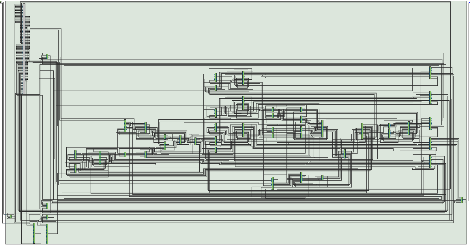
Fig 5. RTL Viewer of Hardware
②Custom IP
The custom IP of puf_sm4 in this design contains the hardware logic of PUF and sm4. The top-level file writes the Avalon interface code to read and write the internal hardware logic of the NiosII Processor.
The custom IP of RTL Viewer is shown in Figure 6:
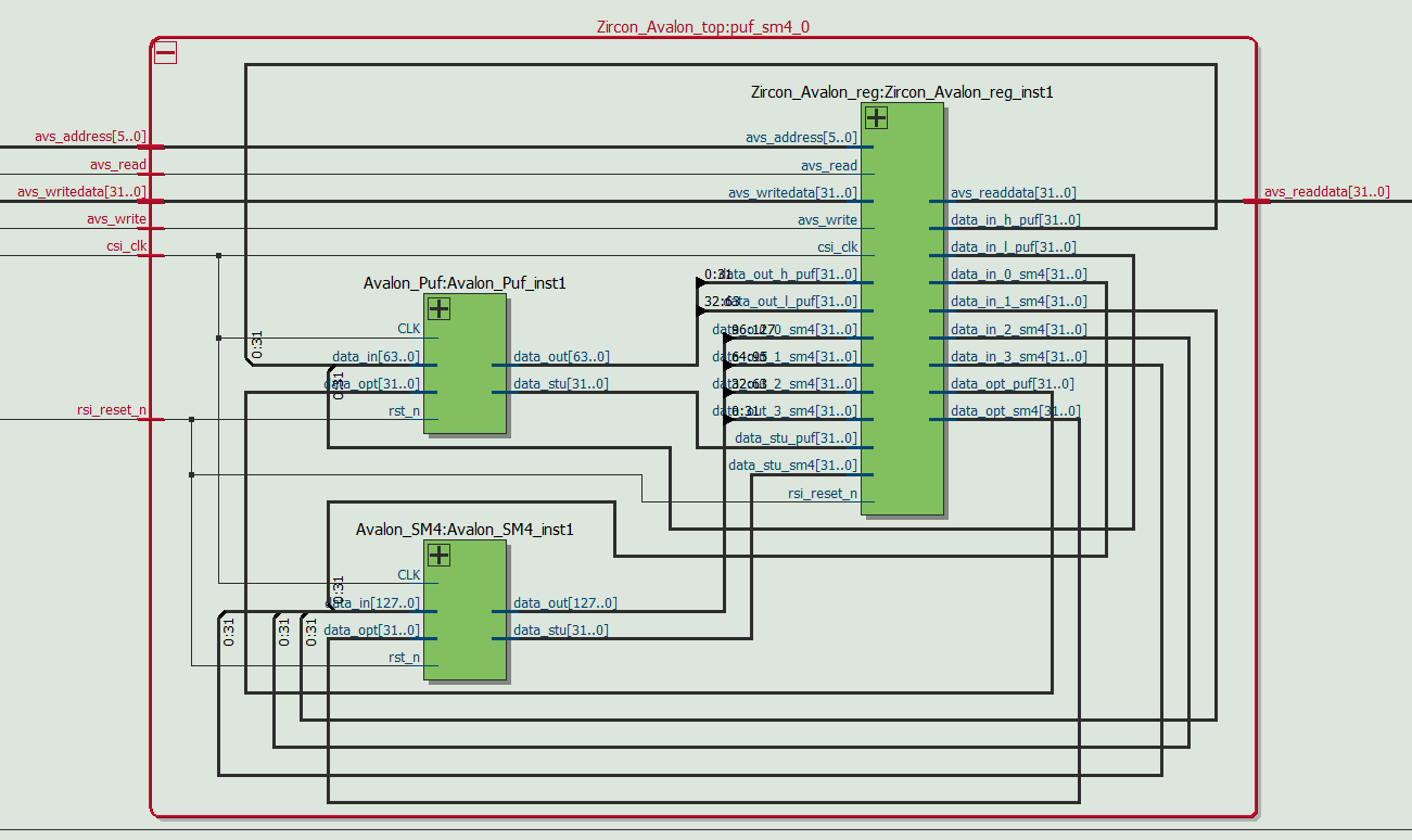
Fig 6. RTL Viewer of puf_sm4
Next we briefly introduce two custom IPs: PUF and SM4.
Figure 7 is a custom IP of PUF circuit structure diagram:
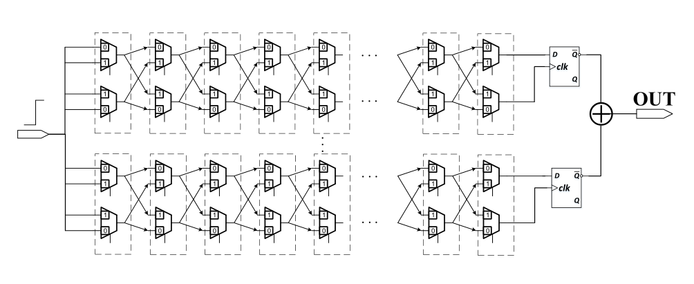 Fig 7. Circuit diagram of PUF
The PUF circuit consists of a delay path and an arbiter located at the end of the delay path. The delay path is composed of multiple nodes, which is composed of two 2:1 MUXs. Two MUXs in each node share a selection control signal. When the control signal is 1, the outputs of the two MUXs of the previous node will be transmitted in parallel to the outputs of the two MUXs of this node. When the control signal is 0, the outputs of the two MUXs of the previous node will be cross-connected to the outputs of the two MUXs of this node. When a transition signal from 0 to 1 enters the delay path, the transition signal will cross or cross each node according to the control signal of each node. If there are n nodes in the delay path, there are totally 2n transmission paths. Finally, after the transition signal is output from the two MUXs at the end of the delay path, it will arrive at the two input terminals of the arbiter. The arbiter outputs 0 or 1 to determine which signal arrives first. The above is the introduction of the basic hardware structure and working principle of the custom IP of PUF.
Figure 8 shows the hardware structure of the custom IP of SM4:
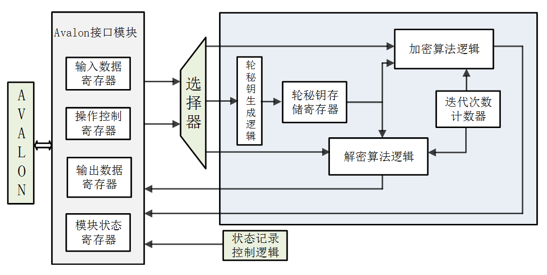
Fig 8. Circuit diagram of PUF
The main core module of the SM4 module is composed of the implementation logic of the SM4 algorithm. There are two main sub-modules in this custom IP: round key generation module and encryption/decryption module. The round key generation module is actually the implementation logic of the key expansion algorithm. It is to perform logical operations on the key, generate round keys, and save them in internal registers. The encryption/decryption module is mainly to process the data logically and obtain the corresponding output data.
⑵A brief introduction and illustration of the upper computer
The upper computer used in this design is designed by our teammate based on MATLAB. The upper computer communicates with the hardware system by UART. Then we can read and write the system through the upper computer to complete PUF operation, encryption and decryption.
Figure 9 is a functional diagram of the upper computer:
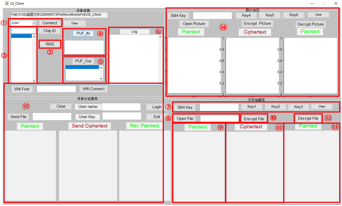
Fig 9.Introduction of upper computer
The following is a brief introduction of each function module:
①Connection: Set the connection port and connection button.
②Random number button: Click this button to automatically generate 32 sets of random numbers and display them in the random number display window.
③Random number display window: The generated random number will be displayed in this window.
④PUF input window: You can input 64 bits of data in this window as an incentive for PUF operation. Data can be randomly combined with random numbers or can be customized. After the data is inputted, click the “PUF_IN” button to send to the Lower machine.
⑤PUF output window: After the lower machine operation is completed, the result of operation will be transmitted to the upper computer and displayed in the window.
⑥Session window: Displays the current working status and warnings.
⑦Key window: In the window you can enter the result of the PUF operation as a key, which is best way. You can also use the preset key "key1, key2, key3" or custom key. After completing the key setting, click the button "SM4 Key" to send the key to the lower machine.
⑧Select encrypted file window: Click on the "Open File" button for file selection. The file will be transmitted to the lower machine and the path of the file will be displayed in the bar window. The content of the file to be encrypted will be displayed in the window.
⑨File to be encrypted window: It will show the contents of the file to be encrypted.
⑩Encryption button: After clicking the “Encrypt File” button, the encryption command is transmitted to the lower machine, and the lower machine starts encryption.
⑪Encryption result output window: When the lower machine encryption is completed, the encrypted data will be transmitted to the upper machine and displayed in this window.
⑫Decryption button: After clicking the button "Decrypt File", the decryption command is transmitted to the lower machine, and the lower machine decrypts the encrypted data.
⑬Decryption result output window: When the decryption of the lower machine is completed, the decrypted data will be transmitted to the upper machine and displayed in this window.
⑭Picture Encryption and Decryption Module: This module is mainly used to encrypt and decrypt pictures. The main workflow is similar to the file encryption and decryption module, so we will not go into details here.
⑮Signature verification module: This module includes WiFi communication, device signature and equipment verification function. At present, the design of this module has not been completed, so we will not go into details here.
Custom IP of PUF performance analysis
The custom IP of PUF used in this design belongs to the group's independent design. After completing the IP design, we test the PUF's custom IP by borrowing third-party tools. Through the third party tools to read and write IP operations, and then get the PUF calculation results. Analysis of PUF Operation Results as shown in Figure 8, Figure 9:
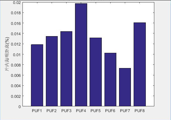
Fig 7. On-chip Hamming distance of random 8 PUFs
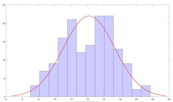
Fig 8. On-chip Hamming distance density distribution
The analysis results show that this custom IP of PUF has great uniqueness and stability, and can achieve the desired protection effect.
⑴ Current system block diagram
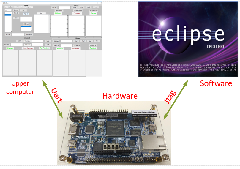
Fig 9. Current system block diagram
⑵ Current system hardware block diagram
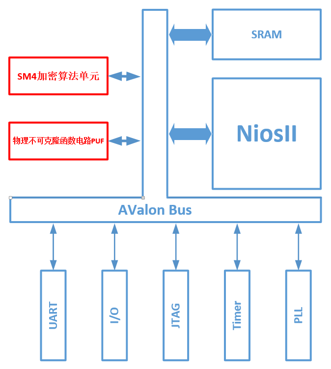
Fig 9. Current system hardware block diagram
⑶ Current system software flow chart
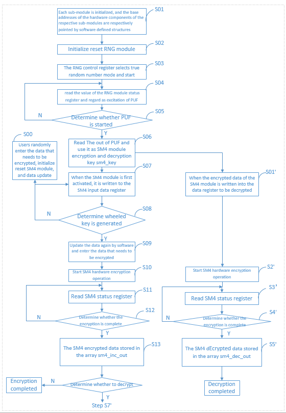
Fig 10. Current system software flow chart