
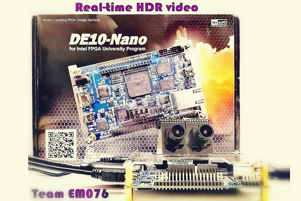
EM076 » Real-time HDR video
We are aimed at making a device for shooting real-time HDR (High Dynamic Range) video using FPGA. Our idea is to simultaneously use two image sensors with different exposure. FPGA receives streams from cameras, uses mathematical algorithms to combine them and transmit HDR video by HDMI.
FPGA enable you to make this process more efficient than CPU thanks to implementation of both the parallel architecture and pipelines.
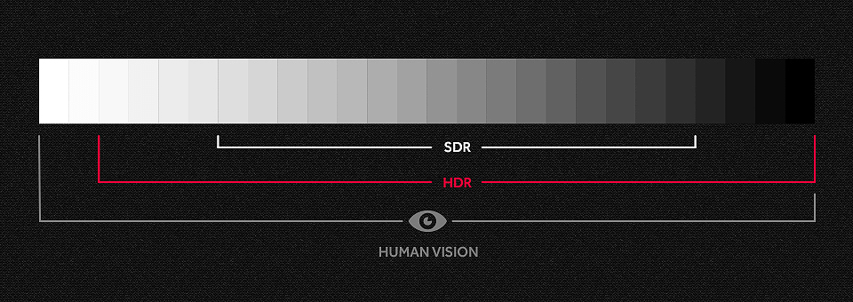
The main idea of our work is application of HDR technology to improve color reproduction quality while video streams, displayed on the monitor in the real time, when shooting of video in backlight (the light source is behind the subject), shooting objects located in different light zones (shadow/intensive light), shooting fast moving objects.
To implement HDR real time video technology, excluding disadvantages, that are presented at a method a single camera used, we chose two identical cameras to shoot video simultaneously, but with different exposure (1st is low, 2nd is high).
Figure 2 shows the Block diagram of the device.
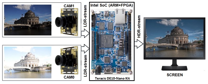
The cameras transmit image to Intel FPGA, where the uniform image is formed by means of mathematical algorithms for data processing. If desired, various filters (edge detechion, blur, black and white, “three-dimensional image”) are applied to the resulting image and the tone correction algorithm is applied.
ARM processor is used to control camera modules, FPGA design and host PC communication, and allows us:
The main idea of HDR real time video producing via FPGA is a parallel data processing. The data comes from two cameras simultaneously. So we need all the calculations is parallel.
Thanks to implementation of both the parallel architecture and pipeline, Intel FPGA enables to make this process more efficient than CPU.
For example, we describe RAW2RGB conversion module in Verilog, then we implement module copies to FPGA, where data from the 0 and 1 cameras are processed. If it's necessary, we can connect 3-4-10 cameras, and even in this case RAW streams from all cameras will be processed and converted to HDR-stream simultaneously.
We have a necessity of application pipeline method for data flow processing. Calculations in modules occur one after another without feedbacks. The modules are also connected one after the other to the pipeline. The data stream is input and set to the output (after some of latency) without interruption.
For example, N-line processed is outputted to the monitor, N+1-line is processed via HDR algorithm, and N+2-line is input and converted from RAW to RGB, - and all these are happen simultaneously.
We have a possibility to rearrange an FPGA design. We can:
All features described are impossible, when the ASIC or CPU are used.
The structure and logic of our project is based on the FPGA virtues, which provide good opportunities to improve the system and algorithms.
It’s possible to expand the project using Intel FPGA. Additional filters can be applied if needed, as well as real-time video.
To Improve the project performance we are going to replace the camera modules with more productive ones and increase their amount. Thanks to FPGA features, there is no need to rebuild a PCB, make additional purchases. The only change is to adjust the code of the input module is a connecting to the new sensors.
In today’s world, it is very important to keep up with the times, not to lose sight of significant events, to follow the current news and know what is happening around. Too rare person can be present personally at the place of events and view the happenings, but the technologies of 21st century allow us to receive up-to-date information being at home.
The usual and most informative way for us to observe the outside world is TV reports and video broadcastings from the place of the most significant events. Online broadcasts and live reports can be called the most exciting and fascinating way of observing, for example the start of a new international expedition to the ISS, a football match, a scientific experiment, an observation over animals in wild nature and so on. Of course, the real time view the happenings on the other end of the globe captures us.
Our work on the HDR real-time HD video implementation may successfully used to security systems, dashcams, traffic control cameras, or in caces of streaming objects, moving with a different speed which are located against the light or in different shadows.
The following equipment and tools are used in the project:
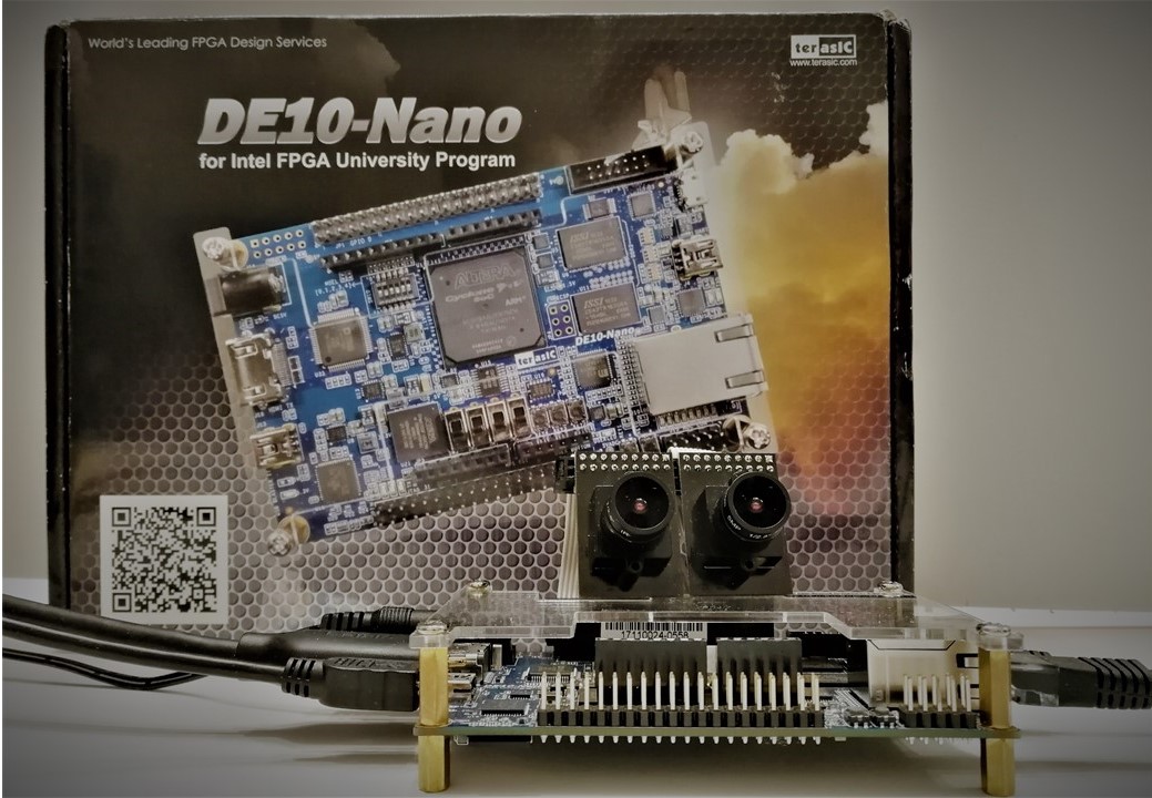
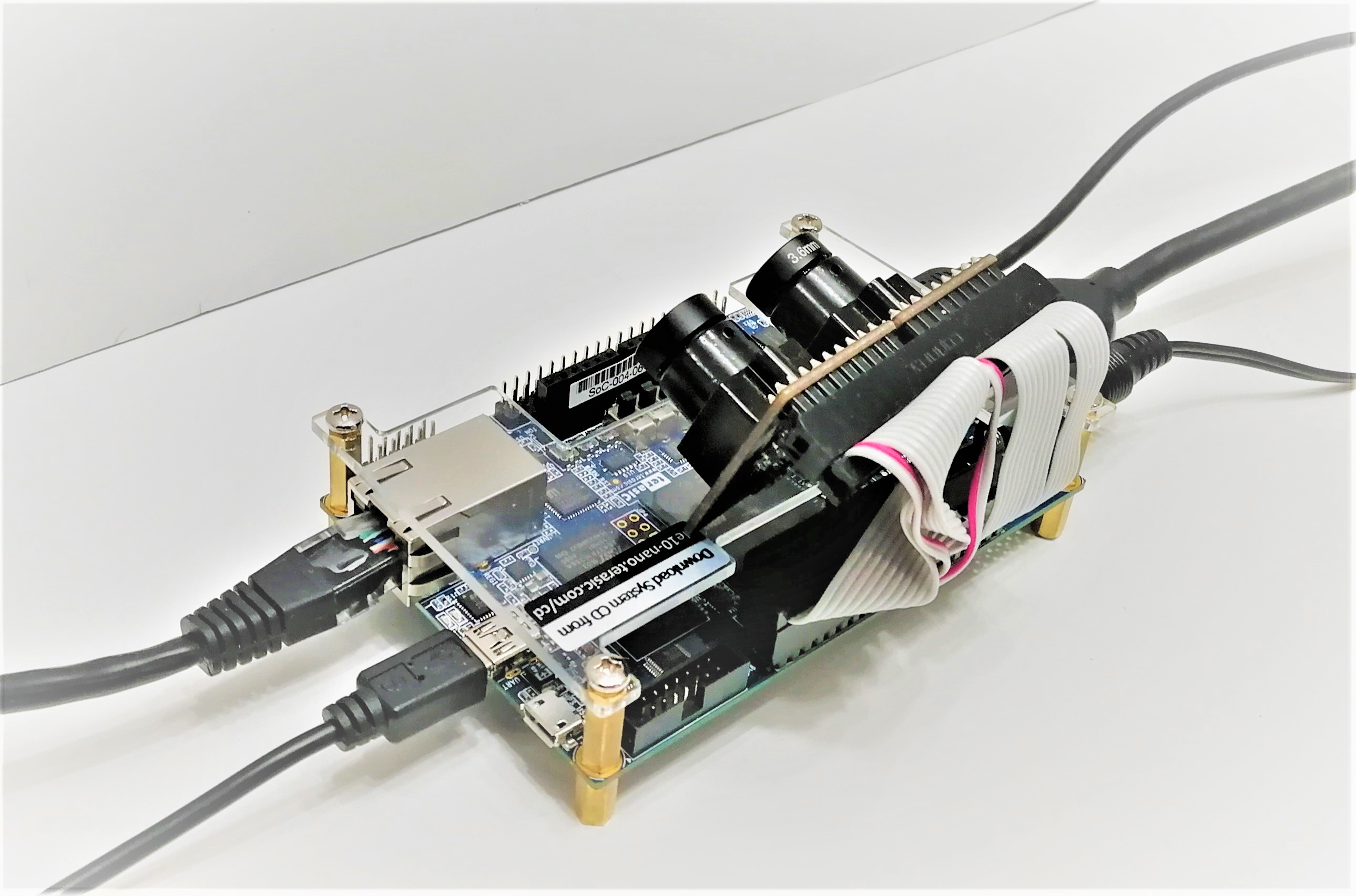
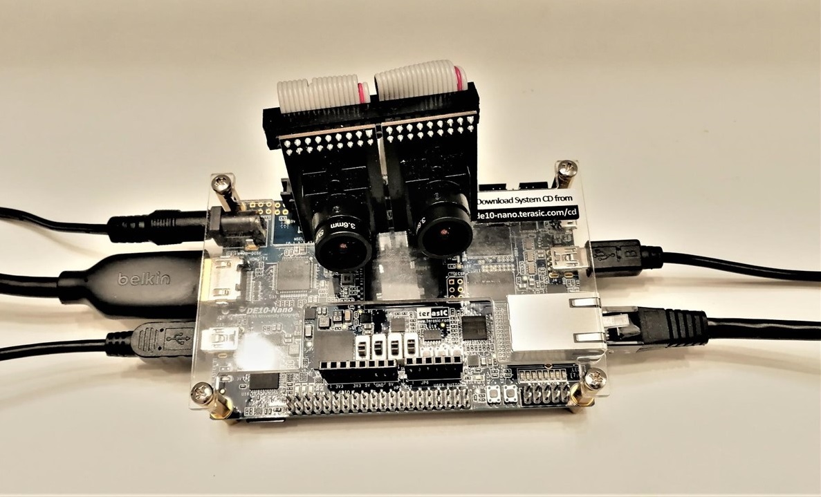
Figure 5 shows the prototype of device.
We use FPGA because of necessity of parallel calculations and pipelining, because it is most benefit this case.
So, our project is based on pipelining:
The functional diagram of FPGA design demonstrating the mutual arrangement of modules is shown on figure 6.
.jpg)
In this architecture ARM doesn’t participate in data processing, the receiver is a monitor, but each frame is registered in shared memory DDR3 access to which has the processor.
Thus, if the process work is required, in our architecture ARM has access to each HDR frame.
When using SoC (FPGA+CPU) we have the opportunity to receive the image with high dynamic range and minimum time delay, available for secondary processing in CPU.
In this project, a 32-bit “hps2fpga” bridge applies to implement external control of video processing and initialization of camera registers. In the address space of this bridge the HPS program transfers transactions to initialize internal FPGA registers or camera control registers. Table 1 lists the addresses of the internal FPGA registers. Parameters from these registers are used for remote control of algorithms for processing the video stream. Transactions received via the hps2fpga bridge with addresses not listed in Table 1 are redirected to the SCCB_camera_config module for conversion to the SCCB interface.
|
|
byte3
|
byte2
|
byte1
|
byte0
|
address
|
|
|
№
|
Name register
|
HPS(offset)
|
FPGA
|
|||
|
1
|
addr_framebuffer_1
|
0x0
|
0x0
|
|||
|
2
|
addr_framebuffer_1
|
0x4
|
0x1
|
|||
|
3
|
|
|
|
hps_switch
|
0x8
|
0x2
|
|
4
|
|
|
|
parallax_corr
|
0xC
|
0x3
|
|
5
|
|
|
|
select_initial_cam
|
0x10
|
0x4
|
|
6
|
|
|
|
div_coef
|
0x14
|
0x5
|
|
7
|
|
|
|
shift_coef
|
0x18
|
0x6
|
|
8
|
|
|
|
matrix_coef[0][0]
|
0x1C
|
0x7
|
|
9
|
|
|
|
matrix_coef[0][1]
|
0x20
|
0x8
|
|
10
|
|
|
|
matrix_coef[0][2]
|
0x24
|
0x9
|
|
11
|
|
|
|
matrix_coef[1][0]
|
0x28
|
0xA
|
|
12
|
|
|
|
matrix_coef[1][1]
|
0x2C
|
0xB
|
|
13
|
|
|
|
matrix_coef[1][2]
|
0x30
|
0xC
|
|
14
|
|
|
|
matrix_coef[2][0]
|
0x34
|
0xD
|
|
15
|
|
|
|
matrix_coef[2][1]
|
0x38
|
0xE
|
|
16
|
|
|
|
matrix_coef[2][2]
|
0x3C
|
0xF
|
|
17
|
|
|
|
start_write_image2ddr
|
0x3fffc
|
0xffff
|
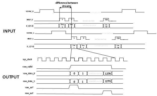
Two asynchronous streams of video data at a frequency of a pixel clock each arrive at the input of the module from gpio pins. The main goal of this module is the synchronization of the two streams with the transition to the system frequency and data output via the avalon_stream interface. The module also counts the difference between HREF strobes. To prevent the increasing of this difference in the gaps between these strobes , the frequency decreases by 1 MHz for that camera, the data from which begin to advance data from another camera by more than the length of one line. This solution ensures stable synchronization of the two streams throughout the entire operation of the camera. An example of the synchronization of the two flows is shown in Fig.7.
even line + even column (for example pixel 7)
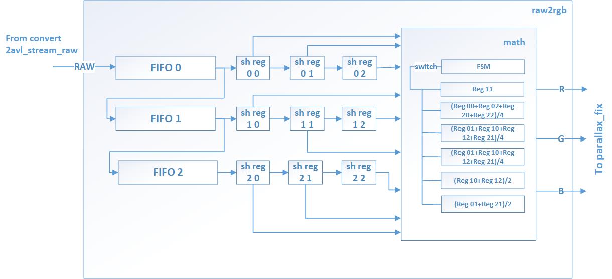
To control switching arithmetic operations the FSM is realized in RAW2RGB DATA PROCESSING MODULE.
To implement the bilinear interpolation method, we need to operate on a 3x3 matrix. To practice this feature in FPGA we use 3 FIFO connected one after another (pipeline).
The input of the first FIFO receives data from camera. FIFO outputs are connected to the shift registers. Thus, the matrix, necessary for calculations, each system clock is in the shift registers.
The latency is the time required to fill 3 FIFOs. After receiving three lines, each system clock new RGB data appears on the output of the RAW2RGB module.
Figure 9 shows the functional scheme of the RAW2RGB module.
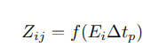
Gamma correction, or often simply gamma, is a nonlinear operation used to encode and decode luminance or tristimulus values in video or still image systems. Gamma correction is, in the simplest cases, defined by the following power-law expression:
It is too difficult to realize calculations of floating-point numbers and exponentiation operations in FPGA, so these operations are realized in CPU.
Gamma correction is realized this way:
Figure 10 shows the Gamma_correction module scheme.
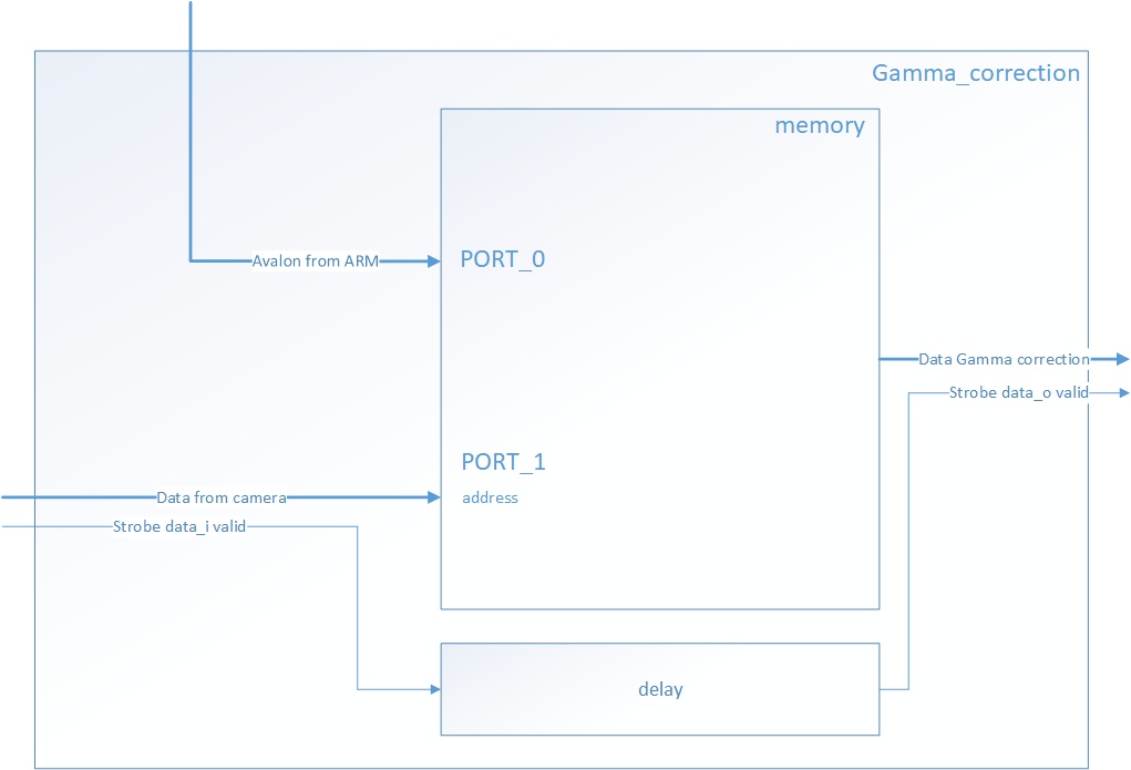
Figure 10. Gamma_correction module scheme
In image processing and photography, a color histogram is a representation of the distribution of colors in an image. For digital images, a color histogram represents the number of pixels that have colors in each of a fixed list of color ranges, that span the image's color space, the set of all possible colors.
Usually, digital camera screen displays shows only brightness histogram (except for expensive SLR cameras), but a color histogram of an image is available only on the computer. Our project enables to construct a real-time color histogram for each color channel, brightness histogram for each camera’s data-stream or for the output stream, at the user's choice.
The histogram construction is divided into 2 parts: FPGA part and CPU part.
A module that contains 256 32-bit registers is described in FPGA. At the beginning of the frame, the registers are set to zero, then the incoming data is analyzed and the register which number is equal to the value on the data bus is incremented.
When the frame is ended, the registers have the values necessary for plotting the histogram.
In C/C++ programming language, a function is implemented that initializes a part of the framebuffer so that a histogram of 200 by 256 pixels is displayed in the lower right corner of the screen.
Figure 11 shows the histogram_module functional scheme.
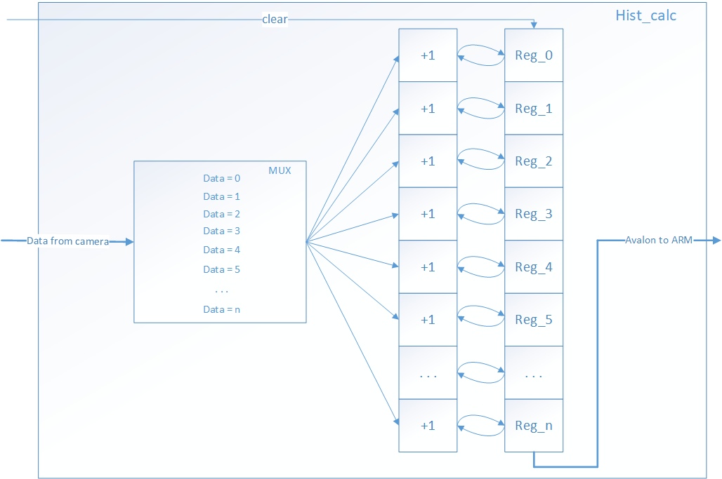
Figure 11. The histogram_module functional scheme
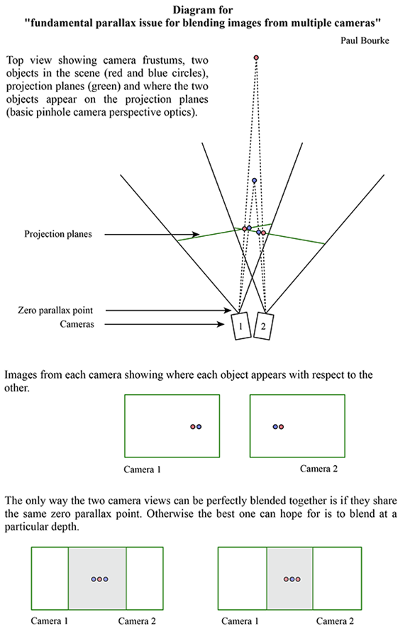
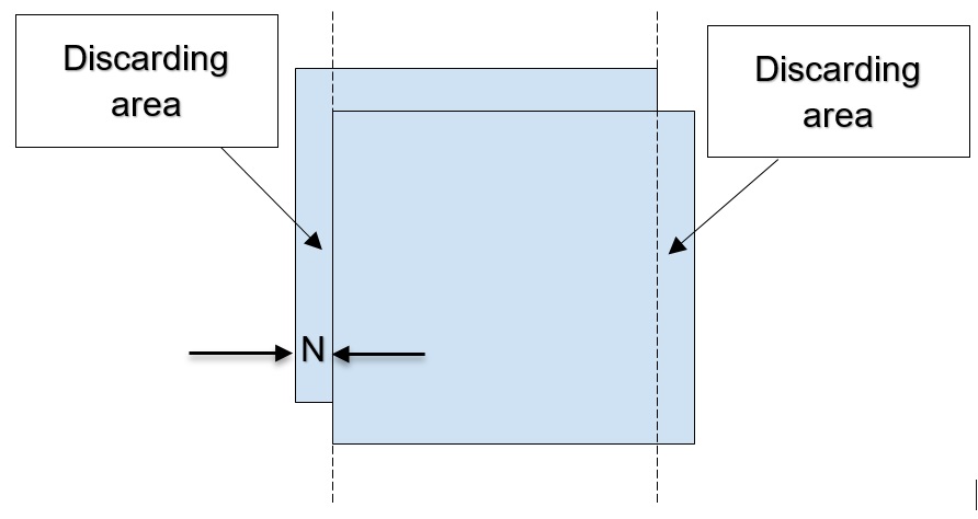
Parallax – changes of visible position of object relative to the distance background in dependence of observer position.
At simultaneous output of images to the monitor from two cameras, which are located as close as possible to each other and adjusted in the angle of elevation and angle of rotation, without processing of incoming data, on the monitor will receive two images with offset relative to each other horizontally. Look at this picture, at least uncomfortable. Figure 12 shows “Fundamental parallax issue for blending images from multiple cameras”.
The Fix_paralax module is implemented to tackle this effect.
Main idea is that the images are displaced to each other, but their biggest areas are intersected, that means that it is necessary to align them. This can be done by discarding the edges of the frame, leaving only the common part of images of two cameras.
Figure 13 shows the two images with offset relative.
In FPGA this method is realized as follows.
On the screen, this appears as a narrow black stripe at the edge of the screen.
For each various constructive execution of such a system, this parameter will have different values, in our case N=50, which is not noticeable when the number of pixels in the line is 1280.
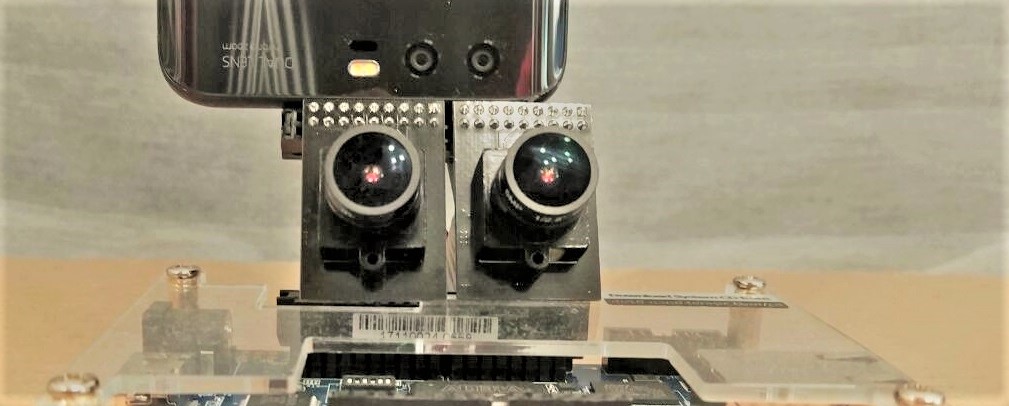 Figure 14. Difference between cameras placing
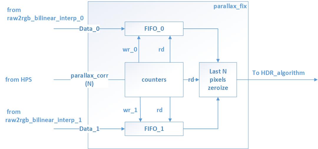
Our project uses inexpensive cameras, which have certain disadvantages, and one of them is the difference in the pixel clock output frequency value.
When the same clock pulse XCLK is applied to the cameras with a frequency of 24 MHz, which is multiplied and divided by the user’s defined values in the internal PLL of the camera module, the frequency of PCLK signals coming from 1 and 2 cameras to the input FPGA are not equal in between. This leads to the fact that processing of each next frame will be out of sync at the time of their admission to the FPGA input. This is unacceptable for our project, as the processing of frames should be synchronized.
To solve this problem, we implemented a frequency tuning algorithm. Its essence is as follows: the time between the beginning of the frame from each camera at the FPGA input is analyzed, the critical value of the time interval difference between the frames is fixed, and at this moment the frequency tuning of the “outrunning” camera is made by reducing the XCLK clock frequency PULSE from 24 down to 23 MHz. When the frames are re-synchronized again on both cameras is fed an XCLK clock frequency 24 MHz.
In this module we use one of the advantages of FPGA - the presence of built-in PLL. Using PLL we can get almost any clock frequency. The ability to operate at different frequencies is important to work with different peripherals, improving performance and reducing energy consumption. Without the ability of the frequency dynamical change on the operating device, our project can not be implemented due to imperfections of the cameras.
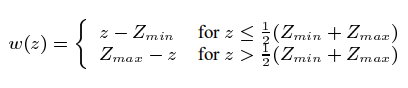
Our work does not imply the creation of a new data processing algorithm to produce HDR, so we used the popular algorithm created by Paul Debevec. The theory of this algorithm can be found in (p. E. Debevec and J. Malik, “Receiving high dynamic range radiance maps from photographs,” in Proceedings of the 24th annual conference on Computer graphics and interactive techniques (SIGGRAPH), 1997, pp. 369-378.).
In this work we have simplified it and implemented it in FPGA. The simplified theory of the above algorithm is presented in the description below.
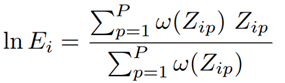
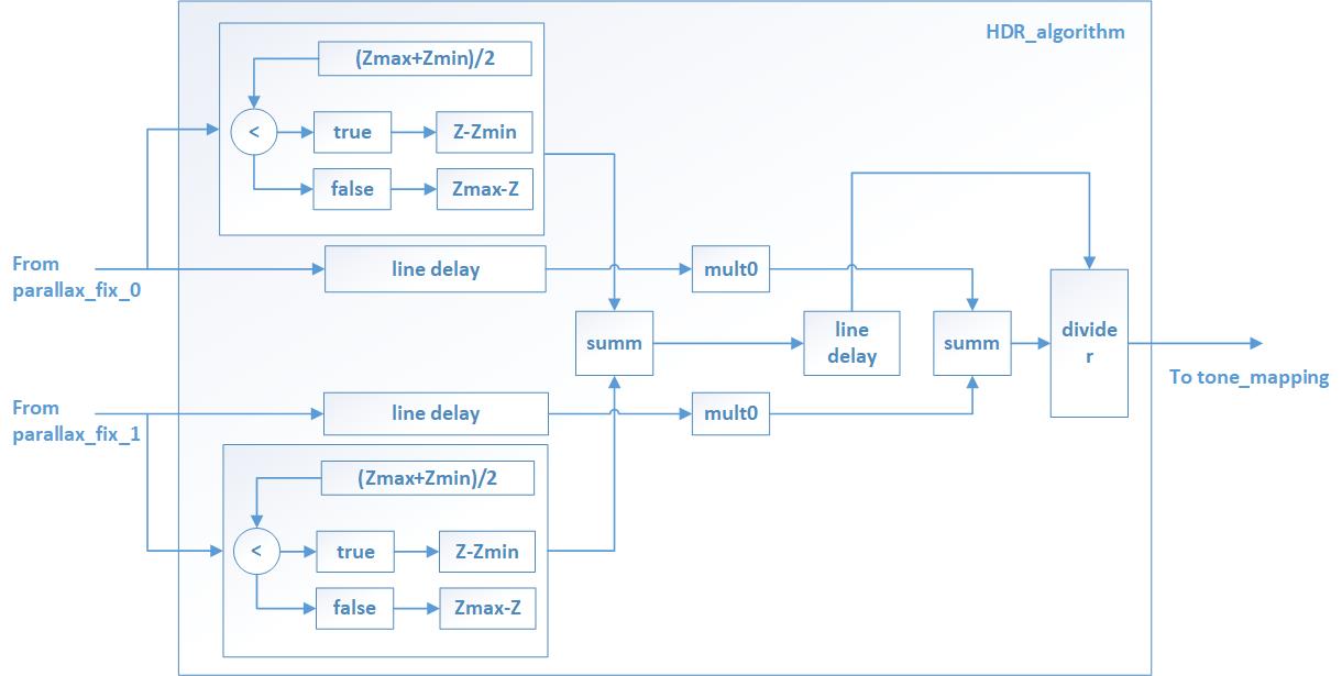
Thus, each tact of the system clock on the module input with the description of the algorithm receives information about the pixel, and each tact of the system clock on the output is set to the value processed by the algorithm.
The advantage of using FPGA in this module is the parallel processing of two data streams: simultaneous calculation of weight coefficients eliminates the need to store data, everything takes place in the stream.
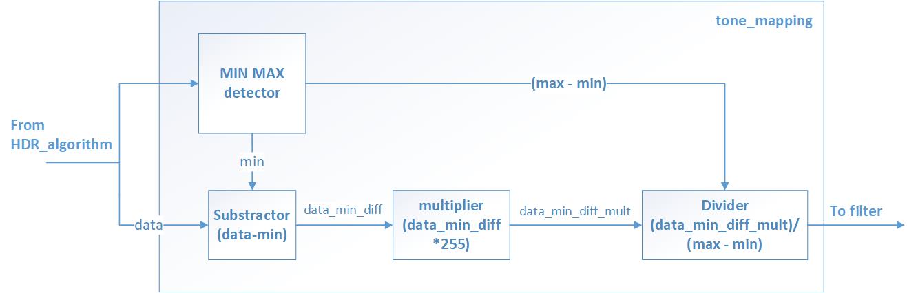
Tone Mapping - is a technique used to convert an image from an extended dynamic range that cannot be represented on a computer monitor screen to a more limited range.
To implement the algorithm, we used the following formula
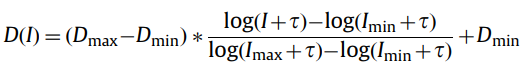
Due to the fact that the video stream is processed in real time, Imin and Imax cannot be used for the current frame, so the assumption is that the brightness between frames does not change dramatically, and the Imin and Imax values for the current frame are taken from the previous one. For the first frame, Imin and Imax are initialized to the minimum and maximum values. Dmin equals 0, Dmax 255, r = 0.
Figure 17 shows the functional diagram of the tone mapping module.
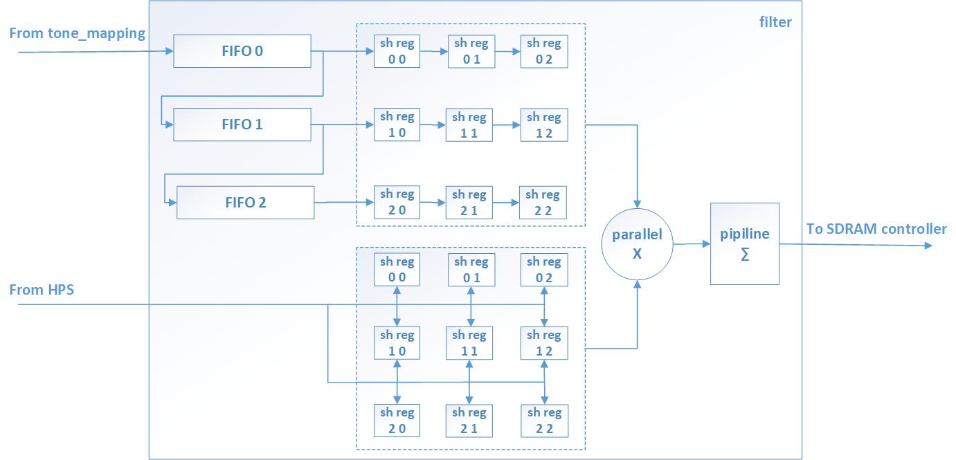
In our project we implemented a filtering module. This module demonstrates the capabilities of the FPGA for stream filtering of the image from noise, obtaining effects such as the presence of edges of objects, blur, sharpen images, etc. These filters are necessary for secondary treatment in CPU in the implementation of the fundamental operations in computer vision, pattern recognition, etc.
The filter implementation algorithm is based on the convolution function. In non-mathematical terms, convolution - is the transformation of one matrix by another, which is called the kernel.
When processing images, matrixes of RGB pixel channels in rectangular coordinates act as the source. Changing the kernel of the matrix, we can get effects such as blur, sharpen, edge detection, emboss and others. Figure 18 shows an example of calculating a single pixel when overlaying a matrix containing a unit at position 01
The calculation of the pixel value is represented in the formula.
(40*0)+(42*1)+(46*0)+(46*0)+(50*0)+(55*0)+(52*0)+(56*0)+(58*0) = 42
In our project we use the kernel of a 3x3 matrix, it is stored in registers and can be updated from HPS. To use the 3x3 kernel, we need to operate with a part of the 3x3 image.
To implement this feature in FPGA we use 3 FIFO connected one after another, the input of the first FIFO receives data from cameras or after HDR processing. The outputs of the FIFO are connected to the shift registers depth 3.
The FIFO’s recording and reading is made simultaneously, and after the first three lines of the FIFO are filled in, the shift registers will have a new value of the 3x3 part of the image. This processing can not be applied to the edges of the image, so we pass them to the output unchanged.
The multiplication of the input image area to the matrix kernel is performed in one clock in 9 parallel multipliers. Summation of multiplication results is organized in a conveyor belt to achieve maximum frequency.
The filter modules are separate for each color component, and the calculations take place in parallel. If necessary, you can apply a filter to a separate color channel.
Figure 19 shows the functional diagram of the filter module
To write any data to the shared memory DDR for HPS and FPGA, it is necessary to allocate a space of continuous physical memory at the Linux kernel level. For this purpose the module of the kernel sdram_module_hdr.ko was written. Аfter insertion into the kernel this module allocates in DDRmemory two buffers.
The size of each buffer - 4 MB. Then the module transfers the initial address of these buffers to write them in the registers of the FPGA with number 1 and 2 into the address space of the bridge hps2fpga.
In this project, the kernel-allocated memory serves as a framebuffer to output the processed HDR video stream to HDMI.
The processed rgb components are written to DDRmemory at the frequency of the camera.
Odd frames are written to the first buffer, even frames are written to the second buffer.
The total number of bytes of a frame required to write a frame is 2764800 bytes. Data transfer is carried out by bursts of length 32 over the bridge fpga2sdram. In total, the transfer of the frame takes 14,400 bursts.
After the current frame is written to the memory buffer, the read module sdram_read is given permission to read the new buffer. Before sending to the SDRAM controller the RGB the components are packed into 64-bit words and written to FIFO to eliminate data loss as a result of the change of signal waitrequest. The format of the 64-bit word is presented in Table 2.
|
Byte7
|
Byte6
|
Byte5
|
Byte4
|
Byte3
|
Byte2
|
Byte1
|
Byte0
|
|
zero
|
b_comp(i+1)
|
g_comp(i+1)
|
r_comp(i+1)
|
zero
|
b_comp(i)
|
g_comp(i)
|
r_comp(i)
|
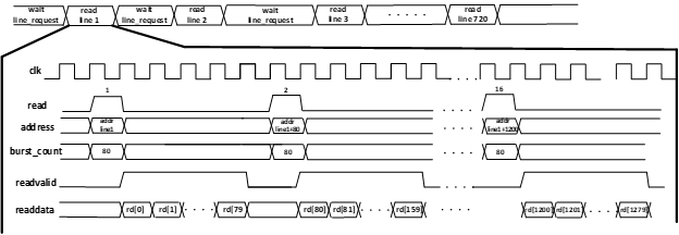
Sending requests for reading a line from DDRmemory begins after receiving from the HDMI_tx signal line_request. The width of the bus of the data interface fpga2sdram_read is 32 bits.
In order to read one line it is necessary to have 16 bursts. Each burst has a length of 80.
The timing diagram for reading data from DDRmemory is shown on the Figure 16. The format of the 32-bit word is given in Table number 3. Switching between buffers in the memory DDRtakes place only after receiving confirmation from the sdram_write module that the new frame is completely loaded into the buffer . Otherwise, the previous frame for the module HDMI_tx will be read again.
|
byte3
|
byte2
|
byte1
|
byte0
|
|
zero
|
b_comp(i)
|
g_comp(i)
|
r_comp(i)
|
Figure 20 shows the timing diagram for reading data.
The ADV7513 High Performance HDMI Transmitter is installed on the Terasic DE0-Nano-SoC developer kit, that allows us not to implement Physical level of HDMI by FPGA. We only need to transmit signals (strobes), which the transmitter requires (HSYNC, VSYNC, DATA ENABLE). It simplifies the implementation of video output on the screen. The necessary information of strobes duration time can be found in CEA-861-E standard.
Figure 21 shows the output waveform of HSYNC, VSYNC, DATA ENABLE.
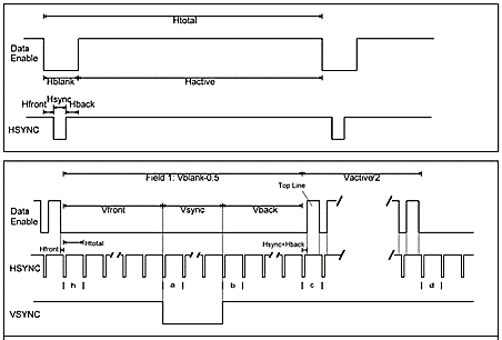
HDMI TX MODULE contains several counters, generating strobes duration required. Before the new line HDMI TX module requests data from the SDRAM controller module to send data to the screen.
This data, received at the system frequency into the HDMI TX module, resync in FIFO HDMI TX to the ADV7513’s necessary frequency and, accompanied by strobes, follow to the ADV7513.
One of the advantage of FPGA, which can be realized in HDMI TX MODULE is the possibility of using another receiver.
We implemented this project with the ADV7513, but, if necessary, it’s possible to transmit video by the other interface, including the physical level (to reassign the input and output pins and voltage standards).
To realize our idea we have employed almost all the elements available in the SoC:
Basically, we can describe these blocks (above) via Verilog manually, but due to the fact that these blocks are realized in SoC (basic), we get a significant system performance advantadges and save resources to implement more other features.
FPGA recources
Figure 22 shows the comparison between the limited/utilized FPGA recources.
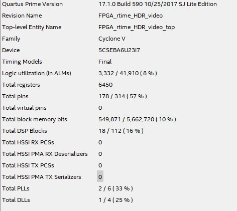
Figure 22. The comparison between the limited/utilized FPGA recources
Resolution (video quality)
We are aimed to get an HD video with 1280x720 resolution. This resolution is chosen to get an optimal "extension/fps" ratio. That was succeed in our project.
Design performance
In our project we use two cameras, getting data according to the waveform below. Figure 23 shows the camera interface data transmitting timing diagram.
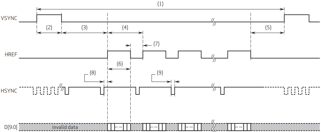
Figure 23. Camera interface data transmitting timing diagram
Data is transmitted in case of “HREF” is high. In case of “HREF” is low the pipeline is out of valid date.
We have measured FPS, using oscilloscope. Figure 24 shows VSYNC pulse period. As we can see, pulse period is 40ms, it means that our system performance is 25 FPS.
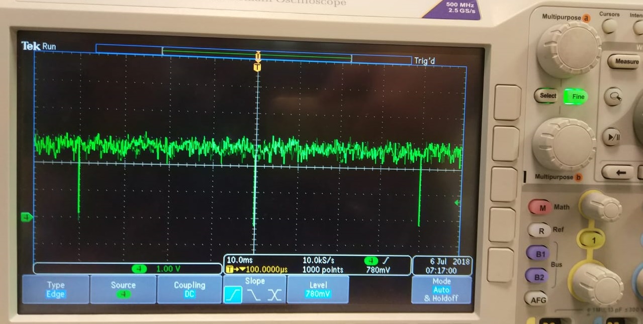
Figure 24. VSYNC pulse period
To estimate the design performance and effectiveness of our project we should consider the ideal case which is not possible while using widely used modern cameras ("HREF" is high always).
In our project FPGA system clock is 100MHz, data bus width from each cameras is 8 bit. Thus, we process the common data stream from two cameras with the speed 1.6 Gb/s.
100*10^6*8*2 = 1.6*10^9bit (1.6 Gb/s)
The one of the main part of our project is to process HD video streams are received from 2 cameras, which is realized not achieved the FPGA performance limit.
We can estimate the FPGA performance limit according to our project.
Time Quest report shows that maximum system clock value of our design is about 130MHz. We can achieve the system clock more than 150MHz via several not difficult optimisations. Thus, we can process the 2.4 Gb/s data stream.
150*10^6*8*2 = 2.4*10^9bit (2.4 Gb/s).
The uniqueness of the project implementation is in the next: nowadays a lot of devices are programmed to get an HDR video using only one camera processing data in CPU.
In our project to realize the HDR real-time HD video we have used two cameras streaming video simultaneosly. The HDR data processing algorithm, we have implemented in the project, is based on the way of several cameras using.
IIn our work this algorithm is realized in FPGA - that is the uniqueness of the project, because the FPGA is not common to aplicate to such tprojects types.
The functional diagram of FPGA design, is demonstrated the mutual arrangement of modules, is shown on figure below (fig.25).
Description
We use two cameras, shooting video simultaneously, but with different exposure (0 camera with low, 1 camera with high).
When the DE-nano10 is ON, “preloader” and “u-boot” run in the ARM.
U-boot updates FPGA firmware and passes control to the Linux kernel, and then the system is ready-to-run. After that, user switches on the User Program. Now the system is ready to use.
Cameras are initialized. Via the “User program”, the necessary data is recorded to the modules on FPGA.
SCCB_camera_config module reads register values and transmits data to the cameras via I2C data protocol.
After cameras are initialized, each camera transmits data to FPGA with different frequencies.
In convert2avl_stream module data streams are resynchronized to the system clock and the starts of frames are synchronized to be able to parallel data processing.
Synchronized data streams are transmitted to gamma_correction modules, where each data stream are corrected not depended.
Corrected data streams are transmitted to the fix_parallax module, where two frames, received from two cameras, are shifted from each other to fix parallax.
The shift value are detected by parallax_corr signal, received from ARM.
Then via RAW2RGB_bilinear_interpolation module RAW data streams are converted to RGB color space.
RGB data streams are transmitted to the HDR module.
Received HDR data stream can be optionally subjected to a tone_mapping module.
In case of indicating bit “enable” as “1”, incoming data streams are processed, in case of indicating bit “enable” as “0”, incoming data streams are not changed.
LDR data streams from the 0 and 1 cameras, and HDR data stream, are transmitted to the MUX1, controlled by the ARM-module. So, we can switch between 2 cameras, or choose the HDR mode.
Data streams are transmitted from MUX1 to the convolution_filter. User chooses the necessary filter, entering coefficients for the convolution matrix kernel. Processed data are transmitted to the SDRAM_write module, which writes Data to DDR3_memory.
Also data from convolution_filter are transmitted to Y_comp module (to calculate brighhtness value from RGB channel) and MUX2, controlled by the ARM-module. So, we can choose necessary histogram: color or brightness.
After user chooses type of histogram, required data stream (Y, R, G, B) is transmitted to the hist_calc module to calculate histogram, values are written to the FPGA+CPU common memory.
The module for data transfer via HDMI - HDMI TX interface requests data from DDR3 memory through the module sdramread and transmits it to the screen.
The main aim of the project is to realize HDR real-time HD video via Terasic DE10-Nano KIT with Intel SoC (FPGA Cyclone V + ARM A9), that is succeed.
Also we have realized some features
Release_1 (31/05/2018). Realized functions:
Release_2 (30/06/2018). Realized additional functions:
SoC (FPGA) architecture flexiblility advantadges are encouraged us to work on the project and improve the algorithms and the system, so we are going to improve the project In the near future.
Starting our project, we were aimed to show practical implementation of our idea by Intel FPGA. While realizing the project, it was found, that concept is working. In spite of using cheap cameras, we have a really good result.
Now the FIFA World Cup Russia 2018 is taking place. We and millions people all over the world are watching live broadcast of this Grand event.
Such events are shot via professional cameras with a best characteristics, costing tens of thousands dollars. But even such cameras have significant disadvantages, for example in cases of shooting objects, which are located against the light or low brightness and high brightness zones simultaneously.
Figure 26 shows the screenshot of football match online broadcasting between Costa Rica and Serbia, whic has taken place a sunny day.
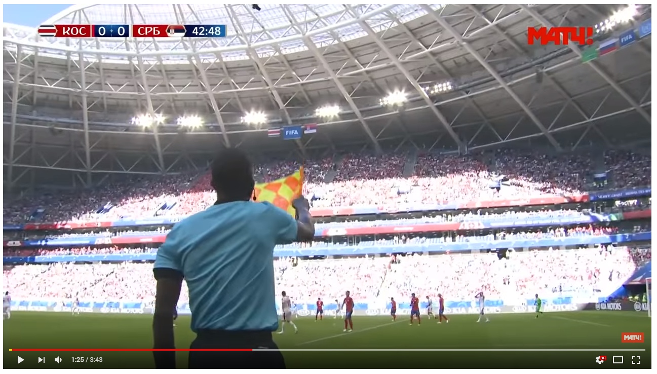
We can see that a lot of details, which are in bright area, are lost in the frame, and this video broadcast was watched by millions spectators.
Figure 27 shows cameras’ dynamic range deficit.
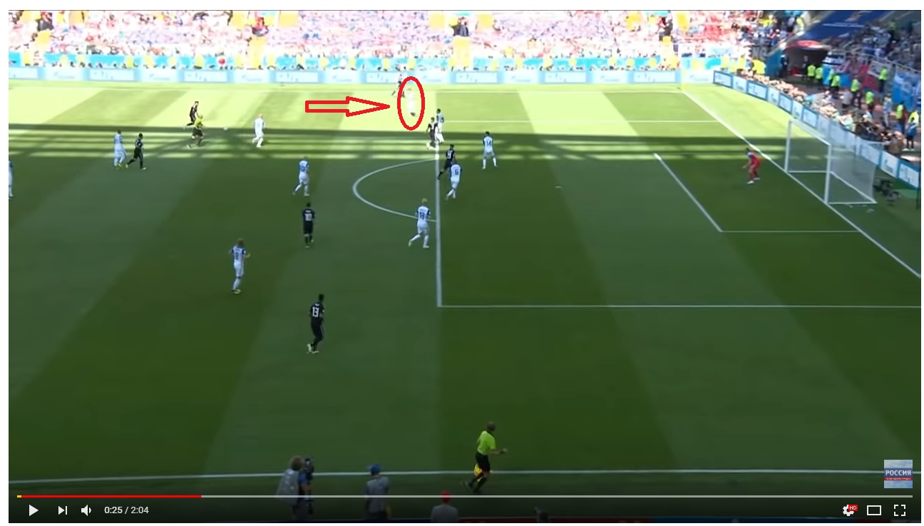
We can see, that football player in white is almost disappeared from the frame, so the viewer can miss important moments of the match.
So, even expencive profeccional premium quality cameras can't fix some problems and transmit high quality real-time HD video, where all areas of frame and every objects are clearly visible.
Areas of our development application are not limited of tasks, which was set at the start of the project, and class of cameras used. Our device is really good if expensive cameras’ using is redundant, for example for high quality selfie-cameras (1 premium quality camera much more expensive than 2 cameras with standard characteristics), as well as good if we want to make live broadcasting with excellent quality when using premium quality camera.
9. Future plans
[1] P. E. Debevec and J. Malik, “Recovering high dynamic range radiance maps from photographs”, 1997.
[2] J. Duan, M. Bressan, C. Dance, and G. Qiu, “Tone-mapping high dynamic range images by novel histogram adjustment,” Pattern Recognition, May 2010.
[4] Dmitry Vatolin “Bayer-pattern interpolation”. Lecture course “Methods of Media data compression”. (RUS: Дмитрий Ватолин "Интерполяция Bayer-pattern". Из курса лекций «Методы сжатия медиаданных»).
